M51995AP/AFP
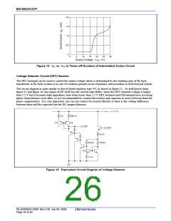
≈ 7.1 V
3 k
500 Ω
1 S
6 S
F/B
−
DET
OP
AMP
+
2.5 V
Figure 16 Equivalent Circuit Diagram of Voltage Detector
ON-OFF Circuit Section
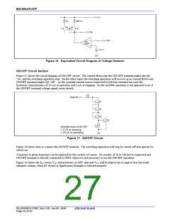
Figure 17 shows the circuit diagram of ON-OFF circuit. The current flown into the ON-OFF terminal makes the Q4
“on” and the switching operation stop. On the other hand, the switching operation will recover as no current flown into
ON/OFF terminal makes Q4 “off”. As the constant current source connected to Q4 base terminal has such the
hysteresis characteristics of 20 µA at operation and 3 µA at stopping. So the unstable operation is not appeared even if
the ON/OFF terminal voltage signal varies slowly.
2 k
ON/OFF
Q1
Q2
Q3
Q4
I
Operate stop at Q4 ON
I: 3 µA at stopping
I: 20 µA at operating
Figure 17 ON/OFF Circuit
Figure 18 shows how to connect the ON/OFF terminal. The switching operation will stop by switch-off and operate by
switch-on.
Transistor or photo transistor can be replaced by this switch, of course. No resistor of 30 to 100 kΩ is connected and
ON/OFF terminal is directly connected to GND, when it is not necessary to use the ON/OFF operation.
Figure 19 shows the ICC versus VCC characteristics in OFF state and VCC will be kept at not so high or low but at the
adequate voltage, when R1 shown in Application Example is selected properly.
REJ03D0835-0300 Rev.3.00 Jun 06, 2008
Page 25 of 40

 RENESAS [ RENESAS TECHNOLOGY CORP ]