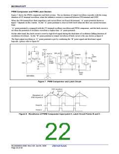
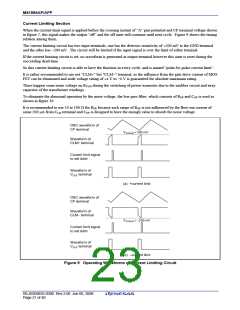
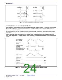
M51995AP/AFP
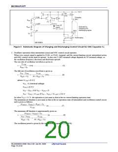
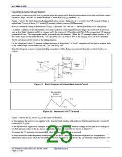
As shown in figure 5, the internal circuit kills the first output pulse in the output waveform. The output waveform
will appear from the second pulse cycle because the duration of first cycle takes CF charging time longer comparing
with that at the stable operating state.
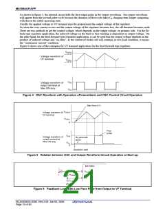
Usually the applied voltage to VF terminal must be proportional the output voltage of the regulator.
So when the over current occurs and the output voltage of the regulator becomes low, the off-duration becomes wide.
There are two methods to get the control voltage, which depends on the output voltage, on primary side. For the fly
back type regulator application, the induced voltage on the third or bias winding is dependent on output voltage. On
the other hand, for the feed forward type regulator application, it can be used that the output voltage depends on the
product of induced voltage and “on-duty”, as the current of choke coil will continue at over load condition, it means
the “continuous current” condition.
Figure 6 shows one of the examples for VF terminal application for the feed forward type regulator.
VOSCH
≈ 4.4 V
Voltage waveform of
CF terminal
VOSCL
≈ 2.0 V
VOH
Voltage waveform of
output terminal at
Max ON duty
VOL
Figure 4 OSC Waveform with Operation of Intermittent and OSC Control Circuit Operation
Start from 0 V
VOSCH
Voltage waveform of
CF terminal
VOSCL
0
First
pulse
VOH
Voltage waveform of
output terminal at
Max ON duty
No generate
pulse
VOL
0
Operation start
Figure 5 Relation between OSC and Output Waveform Circuit Operation at Start-up
M51995A
VOUT
RVFFB
VF
CVFFB
Figure 6 Feedback Loop with Low Pass Filter from Output to VF Terminal
REJ03D0835-0300 Rev.3.00 Jun 06, 2008
Page 19 of 40

 RENESAS [ RENESAS TECHNOLOGY CORP ]