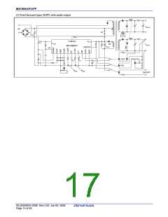
M51995AP/AFP
5.8 V
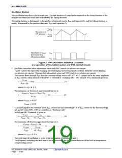
Q4
Q1
1/16
T-ON
Charging
SW1
Q3
RON
ROFF
CF
T-OFF
From VF
signal
Vz = 4.2 V
Switched by
charging and
discharging signal
SW2
CF
Discharging
Q2
M51995A
Figure 3 Schematic Diagram of Charging and Discharging Control Circuit for OSC Capacitor CF
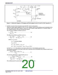
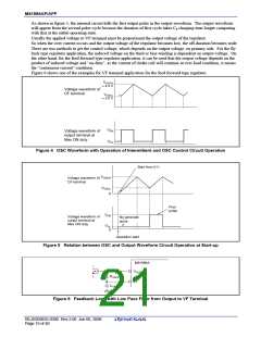
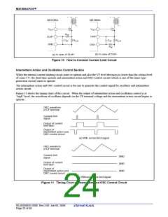
2. Oscillator operation when intermittent action and OSC control circuit operates.
When over current signal is applied to CLM+ or CLM− terminal, and the current limiting circuit, intermittent action
and OSC control circuit starts to operate. In this case T-OFF terminal voltage depends on VF terminal voltage, so
the oscillation frequency decreases and dead-time spreads.
The rise rate of oscillation waveform is given as
VT-ON
≈
(V/s) ………………………………………… (5)
R
ON × CF
The fall rate of oscillation waveform is given as
V
VF − VVFO
VT-ON
≈
+
(V/s) ………………… (6)
R
OFF × CF
16 × RON × CF
where VT-ON ≈ 4.5 V
V
V
V
V
VF ; VF terminal voltage
VFO ≈ 0.4 V
VF − VFO = 0 if VVF − VVFO < 0
VF − VVFO = VT-OFF if VVF – VVFO > VT−OFF ≈ 3.5 V
So when VVF > 3.5 V, the operation is just same as that in the no current limiting operation state.
The maximum on-duration is just same as that in the no-operation state of intermittent and oscillation control circuit
and is given as follows;
(VOSCH − VOSCL) × ROFF × CF
≈
(s) ………………… (7)
VT-ON
The minimum off-duration is approximately given as;
(VOSCH − VOSCL) × CF
≈
(s) ………………… (8)
VVF − VVFO
VT-ON
+
R
OFF × CF
16 × RON × CF
The oscillation period is given by the summation of equation (7) and (8).
REJ03D0835-0300 Rev.3.00 Jun 06, 2008
Page 18 of 40

 RENESAS [ RENESAS TECHNOLOGY CORP ]