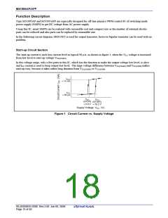
M51995AP/AFP
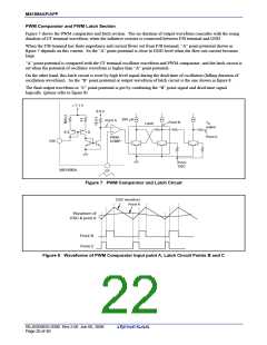
PWM Comparator and PWM Latch Section
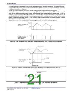
Figure 7 shows the PWM comparator and latch section. The on-duration of output waveform coincides with the rising
duration of CF terminal waveform, when the infinitive resistor is connected between F/B terminal and GND.
When the F/B terminal has finite impedance and current flows out from F/B terminal, “A” point potential shown in
figure 7 depends on this current. So the “A” point potential is close to GND level when the flow-out current becomes
large.
“A” point potential is compared with the CF terminal oscillator waveform and PWM comparator, and the latch circuit is
set when the potential of oscillator waveform is higher than “A” point potential.
On the other hand, this latch circuit is reset by high level signal during the dead-time of oscillation (falling duration of
oscillation waveform). So the “B” point potential or output waveform of latch circuit is the one shown in figure 8.
The final output waveform or “C” point potential is got by combining the “B” point signal and dead-time signal
logically. (please refer to figure 8)
≈ 7.1 V
5.8 V
200 µA
Point A
Point B
To
output
Latch
−
+
6 S
1 S
Point C
PWM
COMP.
F/B
From
OSC
M51995A
CF
Figure 7 PWM Comparator and Latch Circuit
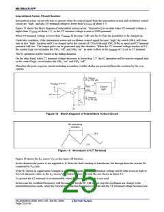
OSC waveform
Point A
Waveform of
OSC & point A
Point B
Point C
Figure 8 Waveforms of PWM Comparator Input point A, Latch Circuit Points B and C
REJ03D0835-0300 Rev.3.00 Jun 06, 2008
Page 20 of 40

 RENESAS [ RENESAS TECHNOLOGY CORP ]