M51995AP/AFP
Oscillator Section
The oscillation waveform is the triangle one. The ON-duration of output pulse depends on the rising duration of the
triangle waveform and dead-time is decided by the falling duration.
The rising duration is determined by the product of external resistor RON and capacitor CF and the falling duration is
mainly determined by the product of resistor ROFF and capacitor CF.
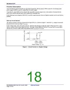
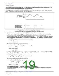
VOSCH
≈ 4.4 V
Waveform of
CF terminal
VOSCL
≈ 2.0 V
Waveform of VOUT
terminal in Max
ON dutycondition
VOH
VOL
Figure 2 OSC Waveform at Normal Condition
(no-operation of intermittent action and OSC control circuit)
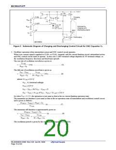
1. Oscillator operation when intermittent action and OSC control circuit does not operate
Figure 3 shows the equivalent charging and discharging circuit diagram of oscillator when the current limiting
circuit does not operate. It means that intermittent action and OSC control circuit does not operate.
The current flows through RON from the constant voltage source of 5.8 V. CF is charged up by the same amplitude
as RON current, when internal switch SW1 is switched to “charging side”. The rise rate of CF terminal is given as
VT-ON
≈
(V/s) ………………………………………… (1)
R
ON × CF
where VT-ON ≈ 4.5 V
The maximum on duration is approximately given as
(VOSCH − VOSCL) × RON × CF
≈
(s) ………………… (2)
VT-ON
where VOSCH ≈ 4.4 V
OSCL ≈ 2.0 V
V
CF is discharged by the summed-up of ROFF current and one sixteenth (1/16) of RON current by the function of Q2,
Q3 and Q4 when SW1, SW2 are switched to “discharge side”.
So fall rate of CF terminal is given as
VT-OFF
VT-ON
≈
+
(V/s) ………………… (3)
R
OFF × CF
16 × RON × CF
The minimum off duration approximately is given as
(VOSCH − VOSCL) × CF
≈
(s) …………………… (4)
VT-OFF
ROFF
VT-ON
+
16 × RON
where VT−OFF ≈ 3.5 V
The cycle time of oscillation is given by the summation of equations 2 and 4.
The frequency including the dead-time is not influenced by the temperature because of the built-in temperature
compensating circuit.
REJ03D0835-0300 Rev.3.00 Jun 06, 2008
Page 17 of 40

 RENESAS [ RENESAS TECHNOLOGY CORP ]