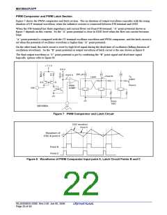
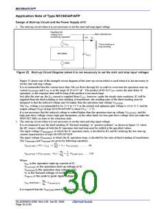
M51995AP/AFP
2.0
1.5
1.0
0.5
0
0
5
10
15
20
25
30
Supply Voltage VCC (V)
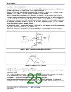
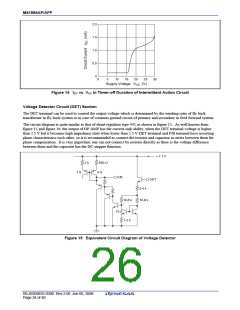
Figure 14 ICC vs. VCC in Timer-off Duration of Intermittent Action Circuit
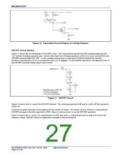
Voltage Detector Circuit (DET) Section
The DET terminal can be used to control the output voltage which is determined by the winding ratio of fly back
transformer in fly-back system or in case of common ground circuit of primary and secondary in feed forward system.
The circuit diagram is quite similar to that of shunt regulator type 431 as shown in figure 15. As well known from
figure 15 and figure 16, the output of OP AMP has the current-sink ability, when the DET terminal voltage is higher
than 2.5 V but it becomes high impedance state when lower than 2.5 V DET terminal and F/B terminal have inverting
phase characteristics each other, so it is recommended to connect the resistor and capacitor in series between them for
phase compensation. It is very important, one can not connect by resistor directly as there is the voltage difference
between them and the capacitor has the DC stopper function.
≈ 7.1 V
3 k
500 Ω
1 S
6 S
F/B
DET
5.4 k
10.8 k
10.8 k
10 S
1.2 k
Figure 15 Equivalent Circuit Diagram of Voltage Detector
REJ03D0835-0300 Rev.3.00 Jun 06, 2008
Page 24 of 40

 RENESAS [ RENESAS TECHNOLOGY CORP ]