3858 Group
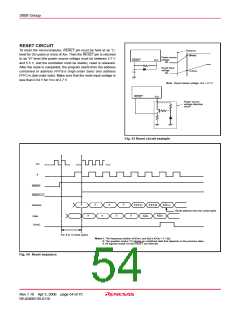
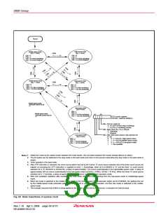
Reset
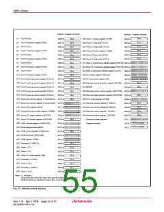
High-speed mode
(f(φ) = 4 MHz)
Middle-speed mode
(f(φ) = 1 MHz)
CM6
CM7 = 0
CM6 = 0
CM7 = 0
CM6 = 1
“1” ←→ “0”
CM5 = 0 (8 MHz oscillating)
CM4 = 0 (32 kHz stopped)
CM5 = 0 (8 MHz oscillating)
CM4 = 0 (32 kHz stopped)
Middle-speed mode
(f(φ) = 1 MHz)
High-speed mode
(f(φ) = 4 MHz)
CM6
CM7 = 0
CM6 = 1
CM5 = 0 (8 MHz oscillating)
CM4 = 1 (32 kHz oscillating)
“1” ←→ “0”
CM7 = 0
CM6 = 0
CM5 = 0 (8 MHz oscillating)
CM4 = 1 (32 kHz oscillating)
Middle-speed mode
automatic switch set bit
"1"
Low-speed mode
(f(φ)=16 kHz)
CM7 = 1
CM6 = 0
CM5 = 0 (8 MHz oscillating)
CM4 = 1 (32 kHz oscillating)
Middle-speed mode
automatic switch start bit
"1"
b7
b4
CPU mode register
(CPUM : address 003B16)
CM
CM
CM
4
5
7
: Port Xc switch bit
0 : I/O port function (stop oscillating)
1 : XCIN-XCOUT oscillating function
: Main clock (XIN- XOUT) stop bit
0 : Operating
1 : Stopped
, CM
6: Main clock division ratio selection bit
Low-speed mode
(f(φ)=16 kHz)
b7 b6
CM7 = 1
CM6 = 0
CM5 = 1 (8 MHz stopped)
CM4 = 1 (32 kHz oscillating)
0
0
1
1
0 : φ = f(XIN)/2 ( High-speed mode)
1 : φ = f(XIN)/8 (Middle-speed mode)
0 : φ = f(XCIN)/2 (Low-speed mode)
1 : Not available
1 : Switch the mode by the allows shown between the mode blocks. (Do not switch between the modes directly without an allow.)
2 : The all modes can be switched to the stop mode or the wait mode and return to the source mode when the stop mode or the wait mode is
ended.
Notes
3 : Timer operates in the wait mode.
4 : After STP instruction is released, the count source which had set by bit 2 (timer 12 count source selection bit) of the timer count source set
register at executing the STP instruction is supplied to timer 1. Accordingly, when bit 0 of MISRG is “0” and the timer 12 count source
selection bit is “0” (f(XIN)/16 or f(XCIN)/16), a delay of approximately 1 ms occurs automatically in the high/middle-speed mode. A delay of
approximately 256 ms occurs automatically in the low-speed mode (at f(XIN) = 8 MHz, f(XCIN) = 32 kHz). When the timer 12 count source
selection bit is “1” (f(XCIN)), a delay of approximately 16 ms occurs regardless of the operation mode.
5 : Wait until oscillation stabilizes after oscillating the main clock XIN before the switching from the low-speed mode to middle/high-speed
mode.
6 : When the mode is switched to the middle-speed mode by the middle-speed mode automatic switch set bit of MISRG, the waiting time set
by the middle-speed mode automatic switch wait time set bit is automatically generated, and then the mode is switched to the middle-
speed mode.
7 : The example assumes that 8 MHz is being applied to the XIN pin and 32 kHz to the XCIN pin. φ indicates the internal clock.
Fig. 60 State transitions of system clock
Rev.1.10 Apr 3, 2006 page 58 of 75
REJ03B0139-0110

 RENESAS [ RENESAS TECHNOLOGY CORP ]