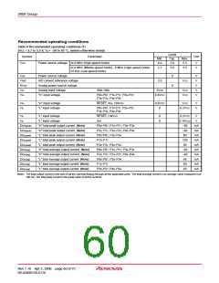
3858 Group
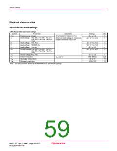
Recommended operating conditions
Table 8 Recommended operating conditions (1)
(VCC = 2.7 to 5.5 V, Ta = –20 to 85 °C, unless otherwise noted)
Limits
Typ.
5.0
Symbol
Parameter
Unit
Min.
4.0
Max.
5.5
VCC
Power source voltage At 8 MHz (High-speed mode)
V
V
At 8 MHz (Middle-speed mode), 6 MHz (High-speed mode)
32 kHz (Low-speed mode)
2.7
5.0
5.5
VSS
VREF
AVSS
VIA
Power source voltage
0
V
V
V
V
V
A/D convert reference voltage
Analog power source voltage
Analog input voltage
2.0
VCC
0
AN0–AN8
AVSS
VCC
VCC
VIH
“H” input voltage
P00–P07, P10–P17, P20–P27,
P30–P34, P40–P44
0.8VCC
VIH
VIL
“H” input voltage
“L” input voltage
RESET, XIN, CNVSS
0.8VCC
0
VCC
V
V
P00–P07, P10–P17, P20–P27,
P30–P34, P40–P44
0.2VCC
VIL
VIL
“L” input voltage
RESET, CNVSS
0
0
0.2VCC
0.16VCC
–80
–80
80
V
“L” input voltage
XIN
V
Σ
Σ
Σ
Σ
Σ
Σ
Σ
Σ
Σ
Σ
IOH(peak)
IOH(peak)
IOL(peak)
IOL(peak)
IOL(peak)
IOH(avg)
IOH(avg)
IOL(avg)
IOL(avg)
IOL(avg)
“H” total peak output current (Note)
“H” total peak output current (Note)
“L” total peak output current (Note)
“L” total peak output current (Note)
“L” total peak output current (Note)
“H” total average output current (Note)
“H” total average output current (Note)
“L” total average output current (Note)
“L” total average output current (Note)
“L” total average output current (Note)
P00–P07, P10–P17, P30–P34
P20, P21, P24–P27, P40–P44
P00–P07, P30–P34
P10–P17
mA
mA
mA
mA
mA
mA
mA
mA
mA
mA
120
80
P20–P27, P40–P44
P00–P07, P10–P17, P30–P34
P20, P21, P24–P27, P40–P44
P00–P07, P30–P34
P10–P17
–40
–40
40
60
P20–P27, P40–P44
40
Note : The total output current is the sum of all the currents flowing through all the applicable ports. The total average current is an average value measured over
100 ms. The total peak current is the peak value of all the currents.
Rev.1.10 Apr 3, 2006 page 60 of 75
REJ03B0139-0110

 RENESAS [ RENESAS TECHNOLOGY CORP ]