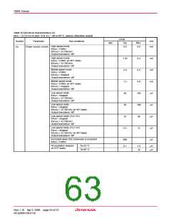
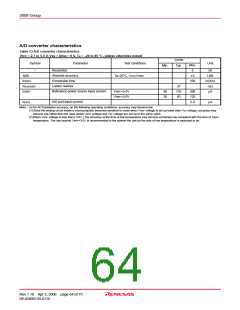
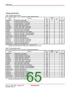
3858 Group
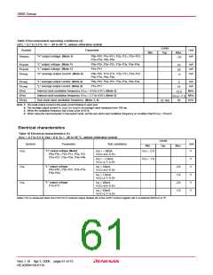
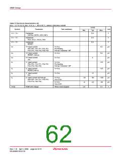
Table 11 Electrical characteristics (2)
(VCC = 2.7 to 5.5 V, VSS = 0 V, Ta = –20 to 85 °C, unless otherwise noted)
Limits
Typ.
0.4
Symbol
VT+ – VT–
Parameter
Unit
V
Test conditions
Min.
Max.
Hysteresis
CNTR0, CNTR1, INT0–INT3
VT+ – VT–
VT+ – VT–
IIH
Hysteresis
RxD, SCLK1, SCLK2, SIN2
0.5
0.5
V
V
Hysteresis
____________
RESET
“H” input current
P00–P07, P10–P17, P20, P21,
P24–P27, P30–P34, P40–P44
VI=VCC
Pin floating,
Pull-up Transistor "off"
5.0
5.0
µA
IIH
IIH
IIL
“H” input current
VI=VCC
VI=VCC
µA
µA
µA
____________
RESET, CNVSS
“H” input current
XIN
4
“L” input current
P00–P07, P10–P17, P20–P27
P30–P34, P40–P44
VI=VSS
Pin floating,
Pull-up Transistor "off"
–5.0
–5.0
IIL
IIL
IIL
“L” input current
VI=VSS
VI=VSS
µA
µA
µA
µA
V
____________
RESET,CNVSS
“L” input current
XIN
–4
“L” input current (at Pull-up)
P00–P07, P10–P17, P20–P27,
P30–P34, P40–P44
VI=VSS
VCC=5.0V
–25
–8
–65
–22
–120
–40
5.5
VI=VSS
VCC=3.0V
VRAM
RAM hold voltage
When clock stopped
2.0
Rev.1.10 Apr 3, 2006 page 62 of 75
REJ03B0139-0110

 RENESAS [ RENESAS TECHNOLOGY CORP ]