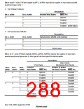
Bit 1—Refresh Mode (RMODE): Selects whether to perform an ordinary refresh or a self-
refresh when the RFSH bit is 1. When the RFSH bit is 1 and this bit is 0, an auto-refresh is
performed on synchronous DRAM at the period set by refresh-related registers RTCNT, RTCOR,
and RTCSR. When a refresh request occurs during an external bus cycle, the refresh cycle is
performed after the bus cycle ends. When the RFSH bit is 1 and this bit is also 1, the synchronous
DRAM will wait for the end of any executing external bus cycle before going into a self-refresh.
All refresh requests to memory that is in the self-refresh state are ignored.
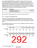
Bit 1: RMODE
Description
0
1
Auto refresh (RFSH must be 1)
Self-refresh (RFSH must be 1)
(Initial value)
Bit 0—Reserved: This bit is always read as 0. The write value should always be 0.
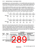
10.2.6 PCMCIA Control Register (PCR)
The PCMCIA control register (PCR) is a 16-bit readable/writable register that specifies the
assertion and negation timing of the OE and WE signals for the PCMCIA interface connected to
areas 5 and 6. The OE and WE signal assertion width is set by the wait control bits in the WCR2
register.
PCR is initialized to H'0000 by a power-on reset, but is not initialized, and retains its contents, in a
manual reset and in standby mode.
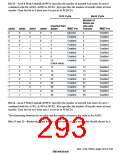
Bit:
15
A6W3
0
14
A5W3
0
13
—
12
—
11
10
9
8
A5TED2 A6TED2 A5TEH2 A6TEH2
Initial value:
R/W:
0
0
0
0
0
0
R/W
R/W
R/W
R/W
R/W
R/W
R/W
R/W
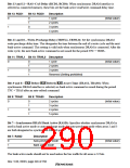
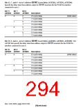
Bit:
7
6
5
4
3
2
1
0
A5TED1 A5TED0 A6TED1 A6TED0 A5TEH1 A5TEH0 A6TEH1 A6TEH0
Initial value:
R/W:
0
0
0
0
0
0
0
0
R/W
R/W
R/W
R/W
R/W
R/W
R/W
R/W
Rev. 5.00, 09/03, page 248 of 760

 RENESAS [ RENESAS TECHNOLOGY CORP ]