10.2.7 Synchronous DRAM Mode Register (SDMR)
The synchronous DRAM mode register (SDMR) is an 8-bit write-only register that is written to
via the synchronous DRAM address bus. It sets synchronous DRAM mode for areas 2 and 3.
SDMR must be set before accessing the synchronous DRAM.
Writes to the synchronous DRAM mode register use the address bus rather than the data bus. If
the value to be set is X and the SDMR address is Y, the value X is written in the synchronous
DRAM mode register by writing in address X + Y. Since, with a 32-bit bus width, A0 of the
synchronous DRAM is connected to A2 of the chip and A1 of the synchronous DRAM is
connected to A3 of the chip, the value actually written to the synchronous DRAM is the X value
shifted two bits right. With a 16-bit bus width, the value written is the X value shifted one bit
right. For example, with a 32-bit bus width, when H'0230 is written to the SDMR register of area
2, random data is written to the address H'FFFFD000 (address Y) + H'08C0 (value X), or
H'FFFFD8C0. As a result, H'0230 is written to the SDMR register. The range for value X is
H'0000 to H'0FFC. When H'0230 is written to the SDMR register of area 3, random data is written
to the address H'FFFFE000 (address Y) + H'08C0 (value X), or H'FFFFE8C0. As a result, H'0230
is written to the SDMR register. The range for value X is H'0000 to H'0FFC.
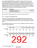
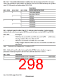
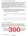
Bit:
31
12
11
—
—
10
—
—
9
8
SDMR address
......................
......................
—
—
W
—
—
W
Initial value:
R/W:
—
—
—
—
*
*
W
W
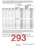
Bit:
7
6
5
4
3
2
1
0
—
—
W
—
—
W
—
—
W
—
—
W
—
—
W
—
—
W
—
—
—
—
—
—
Initial value:
R/W:
Note: * Depending on the type of synchronous DRAM.
Rev. 5.00, 09/03, page 252 of 760

 RENESAS [ RENESAS TECHNOLOGY CORP ]