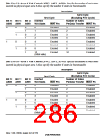
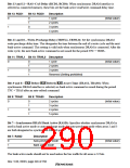
Bits 13 and 12—RAS–CAS Delay (RCD1, RCD0): When synchronous DRAM interface is
selected as connected memory, these bits set the bank active read/write command delay time.
Bit 13: RCD1
Bit 12: RCD0
Description
1 cycle
0
0
1
0
1
(Initial value)
2 cycles
3 cycles
4 cycles
1
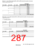
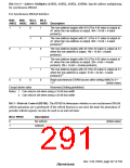
Bits 11 and 10—Write-Precharge Delay (TRWL1, TRWL0): Set the synchronous DRAM
write-precharge delay time. This designates the time between the end of a write cycle and the next
bank-active command. This setting is valid only when synchronous DRAM is connected. After the
write cycle, the next bank-active command is not issued for the period TPC + TRWL.
Bit 11: TRWL1 Bit 10: TRWL0 Description
0
0
1
0
1
1 cycle
(Initial value)
2 cycles
1
3 cycles
Reserved (Setting prohibited)
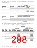
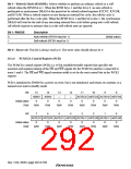
Bits 9 and 8—CAS-Before-RAS Refresh RAS Assert Time (TRAS1, TRAS0): When
synchronous DRAM interface is selected, no bank-active command is issued during the period
TPC + TRAS after an auto-refresh command.
Bit 9: TRAS1
Bit 8: TRAS0
Description
2 cycles
0
0
1
0
1
(Initial value)
3 cycles
1
4 cycles
5 cycles
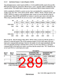
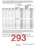
Bit 7—Synchronous DRAM Bank Active (RASD): Specifies whether synchronous DRAM is
used in bank active mode or auto-precharge mode. Set auto-precharge mode when areas 2 and 3
are both designated as synchronous DRAM space.
Bit 7: RASD
Description
0
1
Auto-precharge mode
Bank active mode
(Initial value)
The bank active mode should not be used unless the bus width for all areas is 32 bits.
Rev. 5.00, 09/03, page 246 of 760

 RENESAS [ RENESAS TECHNOLOGY CORP ]