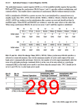
10.2.5 Individual Memory Control Register (MCR)
The individual memory control register (MCR) is a 16-bit readable/writable register that specifies
RAS and CAS timing for synchronous DRAM (areas 2 and 3), specifies address multiplexing, and
controls refresh. This enables direct connection of synchronous DRAM without external circuits.
MCR is initialized to H'0000 by a power-on reset, but is not initialized by a manual reset or in
standby mode. Bits TPC1–TPC0, RCD1–RCD0, TRWL1–TRWL0, TRAS1–TRAS0, RASD, and
AMX3–AMX0 are written to in the initialization after a power-on reset and should not then be
modified again. When RFSH and RMODE are written to, write the same values to the other bits.
When using synchronous DRAM, do not access areas 2 and 3 until this register is initialized.
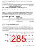
Bit:
15
TPC1
0
14
TPC0
0
13
RCD1
0
12
11
10
9
8
RCD0 TRWL1 TRWL0 TRAS1 TRAS0
Initial value:
R/W:
0
0
0
0
0
R/W
R/W
R/W
R/W
R/W
R/W
R/W
R/W
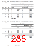
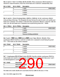
Bit:
7
RASD
0
6
AMX3
0
5
AMX2
0
4
AMX1
0
3
AMX0
0
2
1
0
—
RFSH RMODE
Initial value:
R/W:
0
0
0
R/W
R/W
R/W
R/W
R/W
R/W
R/W
R
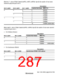
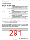
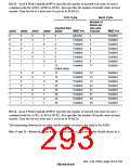
Bits 15 and 14—RAS Precharge Time (TPC1, TPC0): When synchronous DRAM interface is
selected as connected memory, they set the minimum number of cycles until output of the next
bank-active command after precharge. However, the number of cycles input immediately after the
issue of an all-bank-precharge command (PALL) in the case of an auto-refresh or a precharge
command (PRE) in the bank active mode is one fewer than the normal value. TPC1 should not be
set to 0 and TPC0 to 1 in the bank active mode.
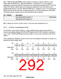
Description
Bit 15:
TPC1
Bit 14:
TPC0
Immediately after
Precharge Command
Immediately after
Self-Refresh
*
Normal Operation
0
0
1
0
1
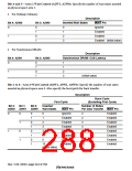
1 cycle (Initial value) 0 cycle (Initial value)
2 cycles (Initial value)
5 cycles
2 cycles
3 cycles
4 cycles
1 cycle
1
2 cycles
3 cycles
8 cycles
11 cycles
Note: * Immediately after all-bank-precharge (PALL) in the case of an auto-refresh or precharge
(PRE) in the bank active mode.
Rev. 5.00, 09/03, page 245 of 760

 RENESAS [ RENESAS TECHNOLOGY CORP ]