Philips Semiconductors
Preliminary specification
Stereo audio codec with SPDIF interface
UDA1355H
handbook, full pagewidth
DATA OUTPUT
BY TRANSMITTER
not acknowledge
DATA OUTPUT
BY RECEIVER
acknowledge
8
SCL FROM
MASTER
1
2
9
S
clock pulse for
acknowledgement
START
condition
MBC602
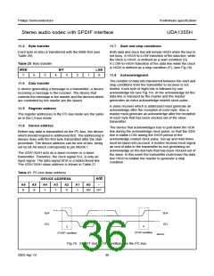
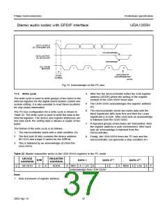
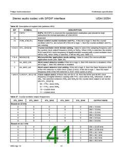
Fig.19 Acknowledge on the I2C-bus.
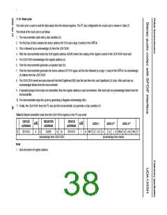
11.9 Write cycle
4. After this the microcontroller writes the 8-bit register
address (ADDR) where the writing of the register
content of the UDA1355H must start.
The write cycle is used to write groups of two bytes to the
internal registers for the digital sound feature control and
system setting. It is also possible to read these locations
for chip status information.
5. The UDA1355H acknowledges this register address
(A).
6. The microcontroller sends two bytes data with the
Most Significant (MS) byte first and then the Least
Significant (LS) byte. After each byte an acknowledge
is followed from the UDA1355H.
The I2C-bus configuration for a write cycle is shown in
Table 22. The write cycle is used to write the data to the
internal registers. The device and register addresses are
one byte each, the setting data is always a couple of two
bytes.
7. If repeated groups of two bytes are transmitted, then
the register address is auto incremented. After each
byte an acknowledge is followed from the
microcontroller.
The format of the write cycle is as follows:
1. The microcontroller starts with a start condition (S).
8. Finally, the UDA1355H frees the I2C-bus and the
microcontroller can generate a stop condition (P).
2. The first byte (8 bits) contains the device address
0011010 and a logic 0 (write) for the R/W bit.
3. This is followed by an acknowledge (A) from the
UDA1355H.
Table 22 Master transmitter writes to the UDA1355H registers in the I2C mode.
DEVICE
ADDRESS
REGISTER
ADDRESS
R/W
DATA 1
DATA 2(1)
.....
DATA n(1)
LSn
S
0011010
0
A
ADDR
A
MS1
A
LS1
A
....
A
A
MSn
A
A
P
acknowledge from UDA1355H
Note
1. Auto increment of register address.
2003 Apr 10
37

 NXP [ NXP ]