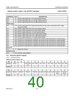
Philips Semiconductors
Preliminary specification
Stereo audio codec with SPDIF interface
UDA1355H
11.3 Byte transfer
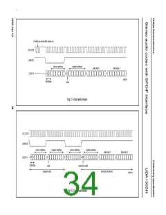
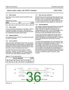
11.7 Start and stop conditions
Each byte (8 bits) is transferred with the MSB first (see
Table 20).
Both data and clock line will remain HIGH when the bus in
not busy. A HIGH-to-LOW transition of the data line, while
the clock is HIGH, is defined as a start condition (S).
A LOW-to-HIGH transition of the data line while the clock
is HIGH is defined as a stop condition (P); (see Fig.18).
Table 20 Byte transfer
MSB
BIT
LSB
7
6
5
4
3
2
1
0
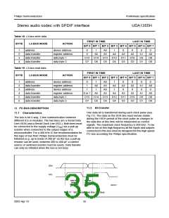
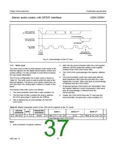
11.8 Acknowledgment
The number of data bits transferred between the start and
stop conditions from the transmitter to receiver is not
limited. Each byte of eight bits is followed by one
acknowledge bit (see Fig.19). At the acknowledge bit the
data line is released by the master and the master
generates an extra acknowledge related clock pulse.
11.4 Data transfer
A device generating a message is a transmitter; a device
receiving a message is the receiver. The device that
controls the message is the master and the devices which
are controlled by the master are the slaves.
A slave receiver which is addressed must generate an
acknowledge after the reception of each byte. Also a
master must generate an acknowledge after the reception
of each byte that has been clocked out of the slave
transmitter.
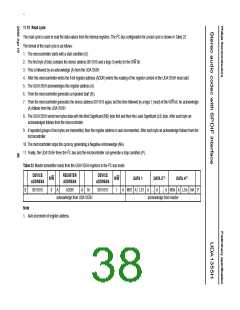
11.5 Register address
The register addresses in the I2C-bus mode are the same
as in the L3-bus mode.
11.6 Device address
The device that acknowledges has to pull-down the SDA
line during the acknowledge clock pulse, so that the SDA
line is stable LOW during the HIGH period of the
acknowledge related clock pulse. Set-up and hold times
must be taken into account. A master receiver must signal
an end of data to the transmitter by not generating an
acknowledge on the last byte that has been clocked out of
the slave. In this event the transmitter must leave the data
line HIGH to enable the master to generate a stop
condition.
Before any data is transmitted on the I2C-bus, the device
which should respond is addressed first. The addressing is
always done with the first byte transmitted after the start
procedure. The device address can be one of two, being
set by bit A0 which corresponds to pin MODE1.
The UDA1355H acts as a slave receiver or a slave
transmitter. Therefore, the clock signal SCL is only an
input signal. The data signal SDA is a bidirectional line.
The UDA1355H slave address is shown in Table 21.
Table 21 I2C-bus slave address
DEVICE ADDRESS
R/W
A6
A5
A4
A3
A2
A1
A0
−
0
0
1
1
0
1
A0
0/1
handbook, full pagewidth
SDA
SDA
SCL
SCL
S
P
STOP condition
START condition
MBC622
Fig.18 START and STOP conditions on the I2C-bus.
2003 Apr 10
36

 NXP [ NXP ]