Philips Semiconductors
Preliminary specification
Stereo audio codec with SPDIF interface
UDA1355H
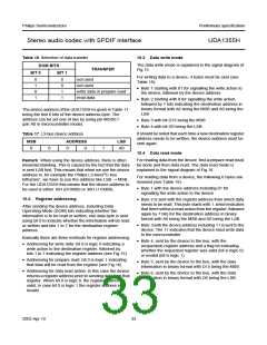
Table 16 Selection of data transfer
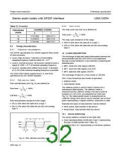
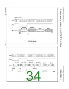
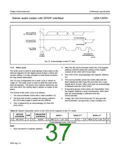
10.3 Data write mode
The data write mode is explained in the signal diagram of
Fig.15.
DOM BITS
TRANSFER
not used
BIT 0
BIT 1
For writing data to a device, 4 bytes must be sent (see
Table 18):
0
1
0
1
0
0
1
1
not used
• Byte 1 starting with 01 for signalling the write action to
the device, followed by the device address
write data or prepare read
read data
• Byte 2 starting with 0 for signalling the write action,
followed by 7 bits indicating the destination address in
binary format with A6 being the MSB and A0 being the
LSB
The device address of the UDA1355H is given in Table 17,
being the first 6 bits of the device address byte. The
address can be set one of two by using pin MODE1
(pin A0 in microcontroller mode).
• Byte 3 with bit D15 being the MSB
• Byte 4 with bit D0 being the LSB.
It should be noted that each time a new destination register
address needs to be written, the device address must be
sent again.
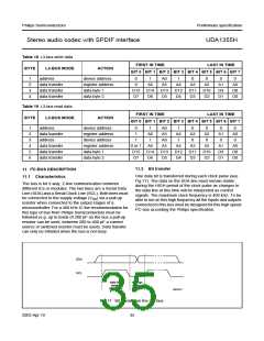
Table 17 L3-bus device address
MSB
ADDRESS
LSB
0
0
0
0
1
A0
10.4 Data read mode
Remark: When using the device address, there is often
misunderstanding. This is caused by the fact that the data
is sent LSB first. This means that when we use the device
address in, for example the Philips L3-bus/I2C-bus
bithacker’, we have to use the address like LSB → MSB.
For the UDA1355H this means that the device address to
be used is either 10H (010000) or 30H (110000).
For reading data from the device, first a prepare read must
be done and then data read. The data read mode is
explained in the signal diagram of Fig.16.
For reading data from a device, the following 6 bytes are
involved (see Table 19):
• Byte 1 with the device address including 01 for
signalling the write action to the device
10.2 Register addressing
• Byte 2 is sent with the register address from which data
needs to be read. This byte starts with 1, which indicates
that there will be a read action from the register, followed
again by 7 bits for the destination address in binary
format with A6 being the MSB and A0 being the LSB
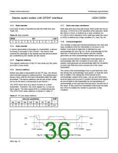
After sending the device address, including Data
Operating Mode (DOM) bits indicating whether the
information is to be read or written, one data byte is sent
using bit 0 to indicate whether the information will be read
or written and bits 1 to 7 for the destination register
address.
• Byte 3 with the device address including 11 is sent to the
device. The 11 indicates that the device must write data
to the microcontroller
Basically there are three methods for register addressing:
• Byte 4, sent by the device to the bus, with the
(requested) register address and a flag bit indicating
whether the requested register was valid (bit is logic 0)
or invalid (bit is logic 1)
• Addressing for write data: bit 0 is logic 0 indicating a
write action to the destination register, followed by
bits 1 to 7 indicating the register address (see Fig.15)
• Addressing for prepare read: bit 0 is logic 1 indicating
that data will be read from the register (see Fig.16)
• Byte 5, sent by the device to the bus, with the data
information in binary format with D15 being the MSB
• Addressing for data read action: in this case the device
returns a register address prior to sending data from that
register. When bit 0 is logic 0, the register address is
valid; in case bit 0 is logic 1 the register address is
invalid.
• Byte 6, sent by the device to the bus, with the data
information in binary format with D0 being the LSB.
2003 Apr 10
33

 NXP [ NXP ]