Philips Semiconductors
Preliminary specification
Stereo audio codec with SPDIF interface
UDA1355H
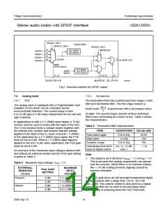
handbook, full pagewidth
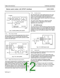
SPDOUT_SEL1
UDA1355H
SPDOUT_SEL0
SPDOUT_SEL2
23
IEC 60958
SPDIF0
[
]
MODE 3:0
DECODER
24
25
26
SPDIF1
SPDIF2
SPDIF3
5
SLICER
SPDIF OUT
select
SPDIF source
IEC 60958
ENCODER
SPDIF
source
21, 22
17 to 19
20
[
]
[
]
SLICER_SEL 1:0
MODE 2:0 SEL_STATIC
MGU833
Fig.6 Selection options for SPDIF output.
7.6
Analog input
ADC
7.6.2
DECIMATION
7.6.1
The decimation from 64fs is performed in two stages: comb
filter and decimation filter. The first stage realizes a
sin x
The analog input is equipped with a Programmable Gain
Amplifier (PGA) which can be controlled via the
microcontroller interface. The control range is from
0 to 24 dB gain in 3 dB steps independent for the left and
right channels.
fourth-order
characteristic with a decimation factor
-----------
x
of eight. The second stage consists of three half-band
filters each decimating by a factor of two. Table 6 shows
the characteristics.
In applications in with a 2 V (RMS) input signal, a 12 kΩ
resistor must be used in series with the input of the ADC.
The 12 kΩ resistor forms a voltage divider together with
the internal ADC resistor and ensures that the voltage,
applied to the input of the IC, never exceeds 1 V (RMS).
In the application for a 2 V (RMS) input signal, the PGA
must be set to 0 dB. When a 1 V (RMS) input signal is
applied to the ADC in the same application, the PGA gain
must be set to 6 dB.
Table 6 Decimation filter characteristics
ITEM
Pass-band ripple
Stop band
CONDITIONS VALUE (dB)
0 to 0.45fs
>0.55fs
±0.02
−60
Dynamic range
0 to 0.45fs
140
Overall gain from ADC DC; VI = 0 dB;
−1.16
input to digital output
note 1
An overview of the maximum input voltages allowed with
and without an external resistor and the PGA gain setting
is given in Table 5.
Note
1. The output is not 0 dB when VI(rms) = 1 V at VDD = 3 V.
This is because the analog components can spread
over the process. When there is no external resistor,
the −1.16 dB scaling prevents clipping caused by
process mismatch.
Table 5 Maximum input voltage; VDD = 3 V
EXTERNAL
RESISTOR
(12 kΩ)
MAXIMUM
INPUT
VOLTAGE
PGA GAIN
SETTING
In the ADC path there are left and right independent digital
volume controls with a range from +24 to −63.5 dB
and −∞ dB. This volume control is also used as a digital
linear mute that can be used to prevent plops when
powering-up or powering down the ADC front path.
Present
0 dB
6 dB
0 dB
6 dB
2 V (RMS)
1 V (RMS)
1 V (RMS)
0.5 V (RMS)
Absent
2003 Apr 10
14

 NXP [ NXP ]