Philips Semiconductors
Objective specification
Integrated PAL and PAL/NTSC TV
processors
TDA8360; TDA8361; TDA8362
SYMBOL
PARAMETER
CONDITIONS
MIN.
TYP.
MAX.
UNIT
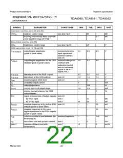
VERTICAL OUTPUT (PIN 43)
IO
available output current
note 7
1
−
−
−
mA
Iint
internal bias current of NPN emitter
follower
−
0.2
mA
VO(max)
VO(min)
maximum available output voltage
minimum available output voltage
4
−
−
−
V
V
−
0.3
VERTICAL FEEDBACK INPUT (PIN 41)
V41
V41
I41
DC input voltage
2.0
−
2.5
1
3.0
−
V
AC input voltage
V
input current
−
−
15
−
µA
%
%
∆tp
internal pre-correction to sawtooth
note 35
−
3
∆T/∆V
temperature dependency on
amplitude
∆T = 40 °C
−
−
1
VGL
VGH
td
vertical guard switching level with
respect to the DC feedback level;
switching level LOW
−
−
−
−
−1.5
+1.5
−
V
vertical guard switching level with
respect to the DC feedback level;
switching level HIGH
−
V
delay of scan start
power on at 60 Hz
note 36
140
ms
Colour demodulation part
CHROMINANCE AMPLIFIER
ACCcr
ACC control range
26
−
−
−
dB
dB
∆V
change in amplitude of the output
signals over the ACC range
−
2
THRon
HYSoff
threshold colour killer ON
hysteresis colour killer OFF
strong input signal
−30
−
−38
dB
note 7
S/N ≥ 40 dB
−
−
+3
+1
−
−
dB
dB
noisy input signal
ACL CIRCUIT
chrominance burst ratio at which the
ACL starts to operate
2.3
−
2.7
REFERENCE PART
Phase-locked loop; note 37
fCR
catching range
300
−
−
−
Hz
∆ϕ
phase shift for a ±200 Hz deviation of note 7
−
2
deg
the oscillator frequency
March 1994
19

 NXP [ NXP ]