Philips Semiconductors
Objective specification
Integrated PAL and PAL/NTSC TV
processors
TDA8360; TDA8361; TDA8362
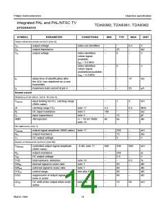
SYMBOL
PARAMETER
CONDITIONS
MIN.
TYP.
MAX.
UNIT
EXTERNAL AUDIO INPUT (TDA8361, TDA8362); NOTE 21 (PIN 6)
V6(rms)
RI
input signal amplitude (RMS value)
input resistance
−
−
−
350
700
mV
25
12
−
−
kΩ
∆GV
voltage gain difference between input maximum volume
and output
dB
αcr
crosstalk between internal and
external audio signals
60
−
−
dB
CVBS/On-Screen Display and CD inputs
INTERNAL AND EXTERNAL CVBS INPUTS (PINS 13 AND 15)
V13(p-p)
internal CVBS input voltage
(peak-to-peak value)
notes 3 and 22
note 3
−
2
2.8
V
I13
internal CVBS input current
−
−
4
1
−
µA
V15(p-p)
external CVBS input voltage;
TDA8361, TDA8362
1.4
V
(peak-to-peak value)
I15
external CVBS input current;
TDA8361, TDA8362
−
4
−
−
µA
ISS
suppression of non-selected CVBS
input signal; TDA8361, TDA8362
note 23
50
−
dB
COMBINED CHROMINANCE AND SWITCH INPUT (TDA8361, TDA8362; PIN 16)
V16(p-p)
chrominance input voltage
(peak-to-peak value)
notes 3 and 24
−
0.3
−
−
V
V
V16(p-p)
input signal amplitude before clipping note 7
occurs (peak-to-peak value)
1
−
RI
chrominance input resistance
−
−
−
15
−
−
kΩ
pF
V
CI
chrominance input capacitance
note 3
5
V16
DC input voltage to switch the
A/V switch to internal mode
−
0.5
V16
DC input voltage to switch the
A/V switch to external mode
VP − 0.5
−
4
−
−
5
−
V
V16
DC input voltage for chrominance
insertion
3
V
SSCVBS
suppression of non-selected
notes 7 and 23
50
dB
chrominance signal from CVBS input
March 1994
15

 NXP [ NXP ]