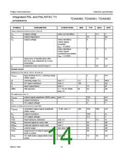
Philips Semiconductors
Objective specification
Integrated PAL and PAL/NTSC TV
processors
TDA8360; TDA8361; TDA8362
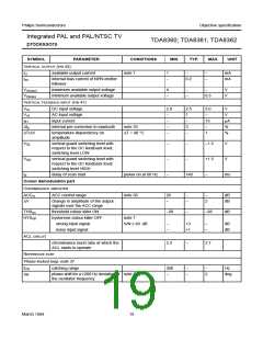
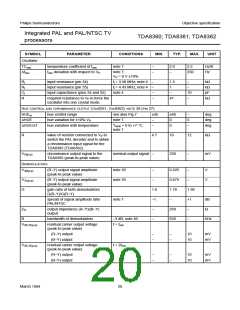
SYMBOL
PARAMETER
CONDITIONS
MIN.
TYP.
MAX.
UNIT
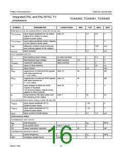
SECOND CONTROL LOOP; NOTE 32 (CAPACITOR CONNECTED TO PIN 39)
∆ϕi/∆ϕo
control sensitivity
without RL on pin 39
−
150
−
−
µs/µs
µs
tcr
control range from start of horizontal
output to flyback
11
12
tshift
maximum horizontal shift range
shift control sensitivity
note 7
note 7
±2
−
−
3
−
−
−
−
µs
∆ϕi/∆ϕo
V39
µA/µs
V
voltage to switch on the X-ray
protection
6
II
input current during protection
−
−
tbf
µA
HORIZONTAL OUTPUT (PIN 37)
VOL
LOW level output voltage
IO = 10 mA
note 7
−
−
0.3
−
V
IO(max)
VO(max)
δdf
maximum allowed output current
maximum allowed output voltage
duty factor
10
−
−
mA
V
−
VP
−
−
50
%
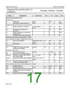
FLYBACK INPUT/SANDCASTLE OUTPUT (PIN 38)
I38
required input current during flyback note 7
100
−
300
µA
pulse
VO
VO
VIcl
tW
output voltage during burst key
output voltage during blanking
clamped input voltage during flyback
burst key pulse width
4.8
1.8
2.6
3.3
−
5.3
2.0
3.0
3.5
14
5.8
2.2
3.4
3.7
−
V
V
V
µs
lines
µs
tW
vertical blanking pulse width
note 33
td
delay of start of burst key to start
of sync
5.2
5.4
5.6
VERTICAL SECTION; NOTE 34
ffr
free running frequency
−
50/60
−
Hz
Hz
flock
locking range
45
−
−
64.5
−
divider value not locked
locking range (lines/frame)
625/525
488
−
722
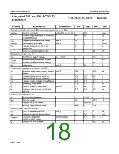
VERTICAL RAMP GENERATOR (PIN 42)
I42
input current during scan
note 7
−
−
−
−
2
µA
mA
V
Idis
discharge current during retrace
0.3
1.5
−
Vsaw(p-p)
sawtooth amplitude
(peak-to-peak value)
in 50 Hz mode
1.8
td
delay from field-to-field
−
−
1.6
µs
March 1994
18

 NXP [ NXP ]