Philips Semiconductors
Objective specification
Integrated PAL and PAL/NTSC TV
processors
TDA8360; TDA8361; TDA8362
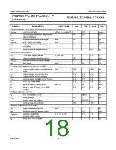
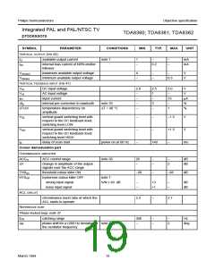
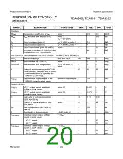
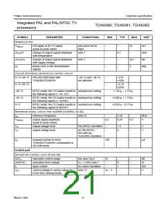
SYMBOL
PARAMETER
CONDITIONS
MIN.
TYP.
MAX.
UNIT
CONTRAST CONTROL; NOTE 25 (PIN 25)
CONcr
contrast control range
see also Fig.9
−
−
20
−
dB
tracking between the three channels
over a control range of 10 dB
−
0.7
dB
BRIGHTNESS CONTROL (PIN 17)
BRIcr
brightness control range
see also Fig.10
−
±1
−
V
V
RGB AMPLIFIERS (PINS 18, 19 AND 20)
V18,19,20(p-p)
output signal amplitudes
(peak-to-peak value)
nominal luminance
input signal and
nominal contrast;
note 25
3.5
4.0
4.5
V20(p-p)
output signal amplitudes for the RED nominal settings for 3.8
4.2
4.6
V
channel (peak-to-peak value)
contrast and
saturation control
and no luminance
signal to the R−Y
signal (PAL)
V18,19,20
V18,19,20
Vpwl
blanking level at the RGB outputs
black level at the RGB outputs
maximum peak white level
available output current
0.5
1.2
−
0.6
1.3
6
0.8
1.4
−
V
note 25
note 42
V
V
IO
5
−
−
mA
Ω
ZO
output impedance
−
150
2.0
−
−
Isource
current source of output stage
1.8
−
−
mA
%
relative spread between the RGB
output signals
5
S/N
signal-to-noise ratio of output signals note 43
for RGB input
for CVBS input
note 7
note 7
−
60
56
−
−
dB
dB
mV
50
−
−
fres(p-p)
fres(p-p)
residual frequency at fosc in the RGB note 23
outputs (peak-to-peak value)
25
residual frequency at 2fosc plus
higher harmonics in the RGB outputs
(peak-to-peak value)
−
−
−
−
25
mV
mV
Vdiff
difference in black level between the nominal brightness
three outputs
100
Vbl
black level shift with picture content
note 7
note 7
−
0
−
mV
∆bl/∆T
variation of black level with
temperature
−2
−
0
mV/K
March 1994
22

 NXP [ NXP ]