Philips Semiconductors
Objective specification
Integrated PAL and PAL/NTSC TV
processors
TDA8360; TDA8361; TDA8362
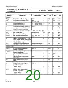
SYMBOL
PARAMETER
CONDITIONS
MIN.
TYP.
MAX.
UNIT
Oscillator
TCosc
temperature coefficient of fosc
fosc deviation with respect to VP
note 7
−
−
2.0
2.5
Hz/K
∆fosc
note 7;
−
250
Hz
VP = 8 V ±10%
RI
RI
CI
R
input resistance (pin 34)
fi = 3.58 MHz; note 4
fi = 4.43 MHz; note 4
note 4
−
−
−
−
1.5
1
−
kΩ
kΩ
pF
kΩ
input resistance (pin 35)
−
input capacitance (pins 34 and 35)
−
10
−
required resistance to VP to force the
oscillator into one crystal mode
47
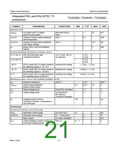
HUE CONTROL AND CHROMINANCE OUTPUT (TDA8361, TDA8362); NOTE 38 (PIN 27)
HUEcr
hue control range
see also Fig.7
note 7
±45
±60
0
−
5
−
deg
deg
deg
∆HUE
hue variation for ±10% VP
hue variation with temperature
−
−
∆HUE/∆T
Tamb = 0 to +7 °C;
0
note 7
R
value of resistor connected to VP to
switch the PAL decoder and to obtain
a chrominance input signal for the
TDA8395 (TDA8362)
4.7
10
12
kΩ
VO(p-p)
chrominance output signal to the
TDA8395 (peak-to-peak value)
nominal output signal −
330
−
mV
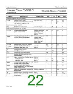
DEMODULATORS
V30(p-p)
(R−Y) output signal amplitude
(peak-to-peak value)
note 39
note 39
−
0.525
0.675
1.78
−
−
V
V
V31(p-p)
G
(B−Y) output signal amplitude
(peak-to-peak value)
−
−
gain ratio of both demodulators
G(B−Y)/G(R−Y)
1.6
−1
−
1.96
+1
−
spread of signal amplitude ratio
PAL/NTSC
note 7
dB
Ω
ZO
output impedance (R−Y)/(B−Y)
output
250
650
B
bandwidth of demodulators
−3 dB; note 40
−
−
kHz
V30,31(p-p)
residual carrier output voltage
(peak-to-peak value)
f = fosc
(R−Y) output
(B−Y) output
−
−
−
−
10
10
mV
mV
V30,31(p-p)
residual carrier output voltage
(peak-to-peak value)
f = 2fosc
(R−Y) output
(B−Y) output
−
−
−
−
10
10
mV
mV
March 1994
20

 NXP [ NXP ]