Philips Semiconductors
Objective specification
Integrated PAL and PAL/NTSC TV
processors
TDA8360; TDA8361; TDA8362
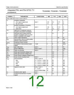
SYMBOL
PARAMETER
CONDITIONS
MIN.
TYP.
MAX.
UNIT
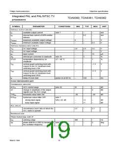
RGB INPUTS FOR ON-SCREEN DISPLAY (PINS 22, 23 AND 24)
V22,23,24(p-p)
input signal amplitude for an output
signal of 4V (black-to-white)
(peak-to-peak value)
note 25
−
0.7
0.8
V
V22,23,24(p-p)
Vdiff
input signal amplitude before clipping
occurs (peak-to-peak value)
1
−
−
−
−
V
difference of black level of internal
and external signals at the outputs
−
100
−
mV
µA
I22,23,24
input currents
0.1
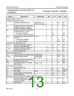
FAST BLANKING (PIN 21)
VI
fast blanking input voltage
no data insertion
data insertion
data insertion
−
−
0.4
−
V
VI
fast blanking input voltage
maximum input pulse
delay of data insertion
input current
0.9
−
−
V
V21(max)
td
−
3
V
−
−
20
−
ns
mA
dB
I21
−
0.2
−
SSint
suppression of internal RGB signals note 23
with data insertion at
46
−
f = 0 to 5 MHz
SSext
suppression of external RGB signals note 23
with data insertion at
f = 0 to 5 MHz
46
4
−
−
−
−
dB
V
VI
input voltage to blank the RGB
outputs to facilitate
note 26
‘On-Screen-Display’ signals being
applied to these outputs
td
delay between the input pulse and
the blanking at the output
note 7
−
30
−
ns
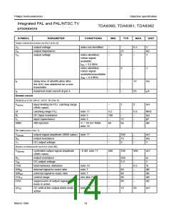
COLOUR DIFFERENCE INPUT SIGNALS (PINS 28 AND 29)
V29(p-p)
V28(p-p)
I28,29
input signal amplitude (R−Y)
(peak-to-peak value)
−
−
−
1.05
1.35
0.1
−
V
input signal amplitude (B−Y)
(peak-to-peak value)
−
V
input current for both inputs
1.0
µA
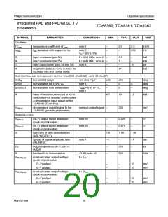
Chrominance filters
CHROMINANCE TRAP CIRCUIT
ftrap
QF
SR
trap frequency
−
fSC
2
−
−
−
MHz
dB
trap quality factor
notes 7 and 27
−
colour subcarrier rejection
20
−
CHROMINANCE BANDPASS CIRCUIT
fc
centre frequency
−
−
fSC
3
−
−
MHz
QBP
bandpass quality factor
note 7
16
March 1994

 NXP [ NXP ]