Philips Semiconductors
Objective specification
Integrated PAL and PAL/NTSC TV
processors
TDA8360; TDA8361; TDA8362
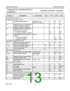
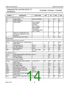
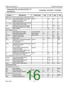
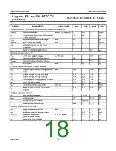
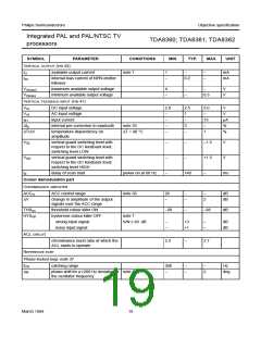
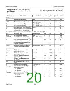
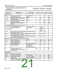
SYMBOL
PARAMETER
CONDITIONS
MIN.
TYP.
MAX.
UNIT
Delay line and peaking circuit
Y DELAY LINE
td
B
delay time
note 7
−
480
−
−
ns
bandwidth of internal delay line
note 7
8
−
MHz
PEAKING CONTROL; NOTE 28, SEE ALSO FIG.6 (PIN 14)
tW
width of preshoot or overshoot
at 50% of pulse;
note 7
−
−
−
−
160
50
1
−
−
−
−
ns
Scth
I14
VI
peaking signal compression
threshold
IRE
mA
V
input current when no video input
signal present
voltage level to switch off peaking
7
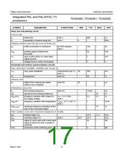
Horizontal and vertical synchronization circuits
SYNC VIDEO INPUT (TDA8361, TDA8362; PINS 13 AND 15)
V13
sync pulse amplitude
referenced to pin 15; 50
note 3
300
50
−
−
mV
%
SL
slicing level
note 29
−
VERTICAL SYNC
tW
width of the vertical sync pulse
without sync instability
note 30
22
−
−
µs
HORIZONTAL OSCILLATOR
ffr
free running frequency
note 44
−
−
−
15625
−
−
Hz
%
∆ffr
spread on free running frequency
±2
∆fosc/∆VP
frequency variation with respect to
the supply voltage
VP = 8 V ±10%;
note 7
0.2
0.5
%
∆fosc/∆T
frequency variation with temperature Tamb = 25 °C ±50 °C;
−
−
1
−
Hz/K
%
note 7
∆fosc( max
)
maximum frequency deviation at the
start of the horizontal output
−
75
FIRST CONTROL LOOP; NOTE 31 (FILTER CONNECTED TO PIN 40)
fHR
fCR
S/N
holding range PLL
catching range PLL
−
±0.9
±0.9
20
±1.2
−
kHz
kHz
dB
note 7
±0.6
−
signal-to-noise ratio of the video input
signal at which the time constant is
switched
−
HYS
hysteresis at the switching point
−
3
−
dB
March 1994
17

 NXP [ NXP ]