Philips Semiconductors
Objective specification
Integrated PAL and PAL/NTSC TV
processors
TDA8360; TDA8361; TDA8362
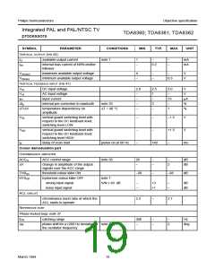
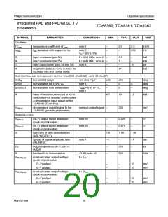
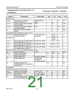
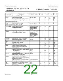
SYMBOL
PARAMETER
CONDITIONS
MIN.
TYP.
MAX.
UNIT
RGB AMPLIFIERS (PINS 18, 19 AND 20)
∆bl/∆CON
∆bl/∆SAT
∆bl
variation of black level over contrast nominal saturation;
−
−
−
−
100
mV
range
note 7
variation of black level over
saturation range
nominal contrast;
note 7
50
mV
relative variation in black level
between the three channels during
variations of
supply voltage (±10%)
saturation (50 dB)
contrast (20 dB)
nominal saturation
nominal contrast
nominal saturation
nominal controls
note 7
−
−
−
−
−
−
−
−
−
−
50
25
60
100
10
mV
mV
mV
mV
mV
brightness (±0.5 V)
Vdiff
B
differential drift of black level over a
temperature range of 40 °C
bandwidth of output signals for
RGB input
−3 dB
8
−
−
8
−
−
−
−
−
MHz
MHz
MHz
MHz
CVBS input
f
osc = 3.58 MHz
2.8
3.5
−
CVBS input
fosc = 4.43 MHz
S-VHS input
Notes to the “Characteristics”
1. It is possible to start the horizontal oscillator when a current of 5.5 mA is supplied to this pin. In this condition the main
part of the IC is not active and this results in the frequency of the oscillator not being controlled at the correct value.
Consequently, the oscillator frequency will be higher than normal, the maximum deviation will be 75%. When the
start-up function is used the maximum voltage on pin 36 must be limited to 8.8 volts.
2. On set AGC.
3. This parameter is not tested during production and is just given as application information for the designer of the
television receiver.
4. Measured at 10 mV RMS top sync input signal.
5. So called projected zero point, i.e. with switched demodulator.
6. Measured in accordance with the test line given in Fig.11. For the differential phase test the peak white setting is
reduced to 87%.
The differential gain is expressed as a percentage of the difference in peak amplitudes between the largest and
smallest value relative to the subcarrier amplitude at blanking level.
The phase difference is defined as the difference in degrees between the largest and smallest phase angle.
7. This parameter is not tested during production but is guaranteed by the design and qualified by means of matrix
batches which are made in the pilot production period.
8. This figure is valid for the complete video signal amplitude (peak white-to-black), see Fig.12.
9. Insertion (suppression of the interference pulses) to a level of 2.6 V is active only during a strong input signal.
This is because the noise inverter has a negative effect on the sound performance at a weak input signal.
10. The test set-up and input conditions are given in Fig.13. The figures are measured with an input signal of
10 mV RMS.
March 1994
23

 NXP [ NXP ]