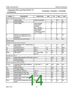
Philips Semiconductors
Objective specification
Integrated PAL and PAL/NTSC TV
processors
TDA8360; TDA8361; TDA8362
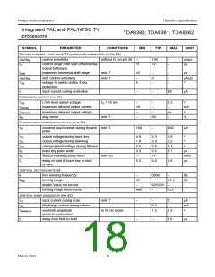
SYMBOL
PARAMETER
CONDITIONS
MIN.
TYP.
MAX.
UNIT
VIDEO IDENTIFICATION OUTPUT (PIN 4)
VO
ZO
VO
output voltage
output impedance
output voltage
video not identified
−
−
−
−
0.5
V
25
6
−
−
kΩ
video identified;
colour signal
available;
V
fosc = 3.5 MHz
video identified;
colour signal
−
8
−
V
available/unavailable
;fosc = 4.4 MHz
td
delay time of identification after
the AGC has stabilized on a new
transmitter
−
−
−
−
10
25
ms
I4
maximum load current at pin 4
µA
Sound circuit
DEMODULATOR INPUT; NOTE 16 (PIN 5)
V5(rms)
input limiting for PLL catching range
−
1
2
mV
(RMS value)
∆f
catching range PLL
DC input resistance
input capacitance
AM rejection
note 17
note 3
note 3
4.2
100
−
−
6.8
−
MHz
kΩ
RI
−
CI
15
66
−
pF
AMR
VI = 50 mV RMS;
note 18
60
−
dB
DE-EMPHASIS (PIN 1)
VO(rms)
RO
output signal amplitude (RMS value) note 17
−
−
−
350
15
3
−
−
−
mV
kΩ
V
output resistance
DC output voltage
V1
AUDIO ATTENUATOR OUTPUT (PIN 50)
V50(rms)
controlled output signal amplitude
−6 dB; note 17
500
700
900
mV
(RMS value)
RO
output resistance
−
−
−
−
−
−
−
250
3.3
−
−
Ω
V50
DC output voltage
−
V
THD
S/Nint
S/Next
VOLcr
OSS
total harmonic distortion
internal signal-to-noise ratio
external signal-to-noise ratio
control range
note 19
0.5
−
%
note 7
60
80
80
80
dB
dB
dB
dB
note 7
−
see also Fig.5
−
suppression of output signal when
mute is active
−
∆V50
DC shift of the output when mute is
active
note 20
−
10
50
mV
March 1994
14

 NXP [ NXP ]