Philips Semiconductors
Objective specification
Integrated PAL and PAL/NTSC TV
processors
TDA8360; TDA8361; TDA8362
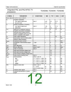
SYMBOL
PARAMETER
CONDITIONS
MIN.
TYP.
MAX.
UNIT
IF AND TUNER AGC; NOTE 12
Timing of IF-AGC (C48 = 2.2 µF)
modulated video interference
30% AM for 1 to
100 mV; 0 to 200 Hz
−
−
−
10
%
tinc
response time for an IF input signal
amplitude increase of 52 dB for
positive and negative modulation
2
−
ms
tdec
response time for an IF input signal
amplitude decrease of 52 dB
for negative modulation
−
−
25
−
−
ms
ms
for positive modulation (TDA8362)
100
Ileak
allowed leakage current of the AGC note 13
capacitor
for negative modulation
for positive modulation
−
−
−
−
10
µA
200
nA
Tuner take-over adjustment (pin 49)
V49(rms)
V49(rms)
Vcr
minimum starting level voltage for
tuner take-over (RMS value)
−
0.2
150
−
0.5
−
mV
mV
V
maximum starting level voltage for
tuner take-over (RMS value)
100
0.5
control voltage range
4.5
Tuner control output (pin 47)
V47
maximum tuner AGC output voltage maximum gain
−
−
−
−
VP + 1
300
V
V47(sat)
output saturation voltage
minimum gain;
I47 = 2 mA
mV
I47
maximum tuner AGC output swing
leakage current RF AGC
5
−
1
−
−
2
−
1
4
mA
µA
dB
Ileak
∆V47
input signal variation for complete
tuner control
IO(max) = 1 mA
AFC OUTPUT; NOTE 14 (PIN 44)
V44
fsl
output voltage swing
−
−
−
−
−
6
−
V
AFC slope
33
−
−
mV/kHz
kHz
V
fos
VO
ZO
AFC offset
note 7
50
−
output voltage at centre frequency
output impedance
3.5
50
−
kΩ
SWITCHING TO POSITIVE MODULATION (TDA8362); NOTE 15 (PIN 1)
V1
minimum voltage on pin 1 to switch
the video demodulator and AGC to
positive modulation
−
−
−
−
VP − 1
V
II
input current
1
mA
March 1994
13

 NXP [ NXP ]