Philips Semiconductors
Objective specification
Integrated PAL and PAL/NTSC TV
processors
TDA8360; TDA8361; TDA8362
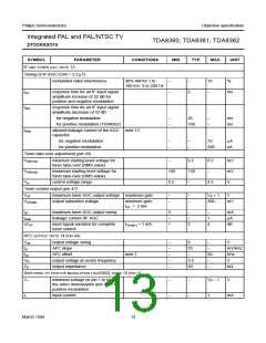
SYMBOL
PARAMETER
CONDITIONS
MIN.
TYP.
MAX.
UNIT
VIDEO AMPLIFIER OUTPUT; NOTE 4 (PIN 7)
V7
negative modulation
zero signal output level
top sync level
note 5
4.45
4.6
4.75
V
1.9
2
2.1
V
V7
positive modulation (TDA8362)
zero signal output level
white level
note 5
1.85
4.2
−
2
2.15
4.4
15
V
4.3
0
V
∆V7
difference in amplitude between
negative and positive modulation
%
V7
detection level of black level for
positive modulation when no peak
white is available in the signal
−
3.1
−
V
ZO
video output impedance
−
−
−
50
Ω
Ibias
internal bias current of NPN emitter
follower output transistor
1
−
mA
Isource
B
maximum source current
−
−
5
mA
bandwidth of demodulated output
signal
−3 dB
6
9
−
MHz
Gdiff
Φdiff
NLvid
Vth
gain differential
note 6
−
−
−
−
−
−
−
2
5
5
5
−
−
−
−
%
deg
%
V
phase differential
video non linearity
white spot threshold voltage level
white spot insertion voltage level
noise inverter clamping voltage level
noise inverter insertion level
intermodulation
notes 6 and 7
note 8
1
−
4.8
3.2
1.4
2.6
Vins
V
Nclamp
Nins
V
note 9
V
δmod
notes 7 and 10
blue
Vo = 0.92 or 1.1 MHz 60
Vo = 0.92 or 1.1 MHz 56
Vo = 2.66 or 3.3 MHz 60
Vo = 2.66 or 3.3 MHz 60
notes 7 and 11
66
62
66
66
−
−
−
−
dB
dB
dB
dB
yellow
blue
yellow
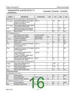
S/N
signal-to-noise ratio
Vi = 10 mV
52
60
61
1
−
−
−
−
dB
end of control range 52
dB
V7
V7
residual carrier signal
note 7
note 7
−
−
mV
mV
residual 2nd harmonic of carrier
signal
0.5
March 1994
12

 NXP [ NXP ]