Philips Semiconductors
Product specification
Multimedia bridge, high performance
Scaler and PCI circuit (SPCI)
SAA7146A
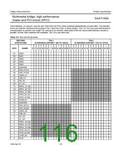
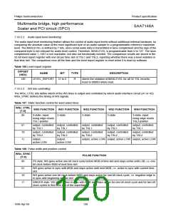
Table 102 Time slot list bit functions
NAME
FUNCTION
WS0
defining pattern of word select signal output at WS0 pin; if WS0 pin is input and trigger, WS0 bit is
meaningless
WS1
WS2
WS3
WS4
defining pattern of word select signal output at WS1 pin
defining pattern of word select signal output at WS2 pin
defining pattern of word select signal output at WS3 pin
defining pattern of word select signal output at WS4 pin: if WS4 pin is input and trigger, WS4 bit is
meaningless
DIS_Ax [1:0]
select serial data input from:
00 : SD0 (for A2); SD4 (for A1)
01 : SD1
10 : SD2
11 : SD3
SDW_Ax
SIB_Ax
SF_Ax
0: do not load this byte into the Dword buffer
1: load this byte into the Dword buffer, place into the next available position
0: do not load this byte into the intermediate feedback buffer
1: load this byte into the intermediate feedback buffer, place into the next available position
0: do nothing
1: store Dword buffer into input FIFO, at the next available position
0: do nothing
LF_Ax
1: load next Dword from output FIFO into output Dword buffer
BSEL_Ax [2:0] select byte for parallel-to-serial converter from output Dword buffer or from intermediate feedback
buffer:
000: take byte 0 from output Dword buffer
001: take byte 1 from output Dword buffer
010: take byte 2 from output Dword buffer
011: take byte 3 from output Dword buffer
100: take byte 0 from intermediate feedback buffer
101: take byte 1 from intermediate feedback buffer
110: take byte 2 from intermediate feedback buffer
111: take byte 3 from intermediate feedback buffer
DOD_Ax [1:0] Define on which SD pin the serial output data will appear: if both circuits attempt to drive the same
SD pin in the same time slot, A1 gets preference. When a SD pin is not driven actively it is 3-stated.
00: at SD0 (for A1); at SD4 (for A2)
01: at SD1
10: at SD2
11: at SD3
LOW_Ax
EOS
Drive the SD pin which was driven in the previous time slot as output: for 7-bit clock cycles to active
LOW and let then go to 3-state.
End Of Superframe: last record in time slot list, next time slot uses first record of the TSL (reset TSL
pointer).
1998 Apr 09
117

 NXP [ NXP ]