OXCB950
OXFORD SEMICONDUCTOR LTD.
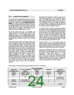
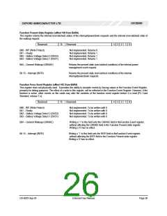
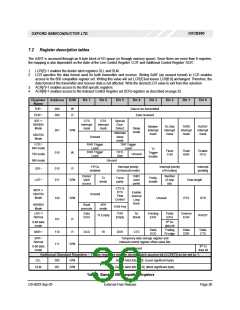
Function Present State Register (offset +08 from BAR4)
This register returns the internal (non-latched) states of the interrupt/powerdown requests and the internal (non-latched) state of
the wakeup request.
Reserved
15 Reserved
4 3 2 1 0
BIt0 - WP (Write Protect).
Not implemented. Returns 0.
Bit1 – Ready.
Not implemented. Returns 1.
Not implemented. Returns 1.
Not implemented. Returns 1.
BIt2 – Battery Voltage Detect 2 (BVD2).
Bit3 – Battery Voltage Detect 1 (BVD1)
Bit4 – General Wakeup (GWAKE)
Returns the present state (non-latched condition) of the internal power
management event request.
Bit 15 – Interrupt (INTR)
Returns the present state (non-latched condition) of the internal
interrupt/powerdown requests.
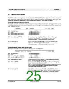
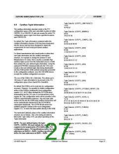
Function Force Event Register (offset +0C from BAR4)
This register does not physically exist. It provides the ability to simulate events by forcing values in the Function Event Register,
primarily for debug purposes. The effect of a write to this register, will be reflected in the Function Event Register. However, if the
function is active, other events on the cards may alter the contents of the function event register before it is read {PC Card
Standard, release 7.x}.
Reserved
15 Reserved
4 3 2 1 0
BIt0 - WP (Write Protect).
Not implemented. To be written with 0.
Bit1 – Ready.
Not implemented. To be written with 0.
Not implemented. To be written with 0.
Not implemented. To be written with 0.
BIt2 – Battery Voltage Detect 2 (BVD2).
Bit3 – Battery Voltage Detect 1 (BVD1)
Bit4 – General Wakeup (GWAKE)
Bit 15 – Interrupt (INTR)
Writing a ‘1’ to this field sets the GWAKE field in theFunction Event register,
without affecting the GWAKE field in the Function Present state register.
Writing a ‘0’ has no effect.
Writing a ‘1’ to this field sets the INTR field in theFunction Event register,
without affecting the INTR field in the Function Present state register
Writing a ‘0’ has no effect.
DS-0033 Sep 05
External-Free Release
Page 26

 OXFORD [ OXFORD SEMICONDUCTOR ]