OXCB950
OXFORD SEMICONDUCTOR LTD.
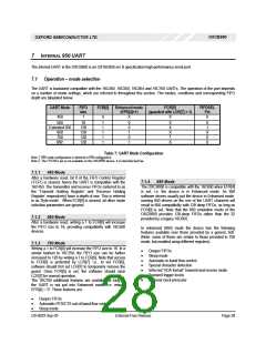
7.1.5 950 Mode
transmitters. FIFO levels are readable using RFL and TFL
registers.
The additional features offered in 950 mode generally only
apply when the UART is in Enhanced mode (EFR[4]=’1’).
Provided FCR[0] is set, in Enhanced mode the FIFO size is
128.
The UART has a flexible prescaler capable of dividing the
system clock by any value between 1 and 31.875 in steps
of 0.125. It divides the system clock by an arbitrary value in
“M+N/8” format, where M and N are 5- and 3-bit binary
numbers programmed in CPR[7:3] and CPR[2:0]
respectively. This arrangement offers a great deal of
flexibility when choosing an input clock frequency to
synthesise arbitrary baud rates. The default division value
is 4 to provide backward compatibility with 16C650
devices.
Note that 950 mode configuration is identical to that of 650
mode, however additional 950 specific features are
enabled using the Additional Control Register ‘ACR’ (see
section 7.11.3). In addition to larger FIFOs and higher baud
rates, the enhancements of the 950 mode over 650
emulation mode are:
•
•
Selectable arbitrary trigger levels for the receiver and
transmitter FIFO interrupts
The user may apply an external 1x (or Nx) clock for the
transmitter and receiver to the RI# and DSR# pin
respectively. The transmitter clock may instead be asserted
on the DTR# pin. The external clock options are selected
through the CKS register (offset 0x02 of ICR).
Improved automatic flow control using selectable
arbitrary thresholds
•
•
•
•
•
•
•
DSR#/DTR# automatic flow control
Transmitter and receiver can be optionally disabled
Software reset of device
It is also possible to define the over-sampling rate used by
the transmitter and receiver clocks. The 16C450/16C550
and compatible devices employ 16 times over-sampling,
where there are 16 clock cycles per bit. However the 950
UART can employ any over-sampling rate from 4 to 16 by
programming the TCR register. This allows the data rates
to be increased to 460.8 Kbps using a 1.8432MHz clock, or
15 Mbps using a 60 MHz clock. The default value after a
reset for this register is 0x00, which corresponds to a 16
cycle sampling clock. Writing 0x01, 0x02 or 0x03 will also
result in a 16 cycle sampling clock. To program the value to
any value from 4 to 15 it is necessary to write this value
into the TCR i.e. to set the device to a 13 cycle sampling
clock it would be necessary to write 0x0D to TCR. For
further information see section 7.10.3
Readable FIFO fill levels
Optional generation of an RS-485 buffer enable signal
Four-byte device identification (0x16C95005)
Readable status for automatic in-band and out-of-
band flow control
•
•
•
External 1x clock modes (see section 0)
Flexible “M+N/8” clock prescaler (see section 7.10.2)
Programmable sample clock to allow data rates up to
15 Mbps (see section 7.10.3).
•
•
9-bit data mode
Readable FCR register
The 950 trigger levels are enabled when ACR[5] is set
where bits 4 to 7 of FCR are ignored. Then arbitrary trigger
levels can be defined in RTL, TTL, FCL and FCH registers
(see section 7.11). The Additional Status Register (‘ASR’)
offers flow control status for the local and remote
The UART also offers 9-bit data frames for multi-drop
industrial applications.
DS-0033 Sep 05
External-Free Release
Page 29

 OXFORD [ OXFORD SEMICONDUCTOR ]