OXCB950
OXFORD SEMICONDUCTOR LTD.
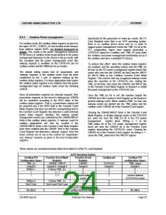
6.7 Cardbus Status Registers
The 4 32-bit cardbus status registers as defined by the tuple CISTPL_CONFIG_CB are detailed below. These are available
when the parameter ‘enable cardbus status registers’ has been enabled in the device’s local configuration register LCC. These
registers are relevant to the cardbus mode of the device and have no meaning for the pci mode of the device.
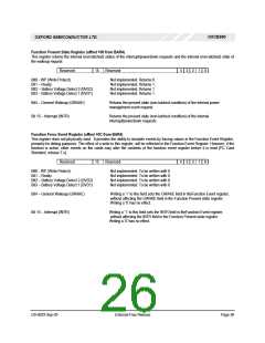
Function Event Register (offset +00 from BAR4)
This register returns the latched states of any internal power management events and internal interrupt/powerdown requests
(which would otherwise have set the device’s interrupt pin and CSYSCHG pin if the corresponding fields in the Function Event
Mask Register are also set)
Reserved
15 Reserved
4 3 2 1 0
BIt0 - WP (Write Protect).
Not implemented. Returns 0.
Not implemented. Returns 0.
Not implemented. Returns 0.
Not implemented. Returns 0.
Bit1 – Ready.
BIt2 – Battery Voltage Detect 2 (BVD2).
Bit3 – Battery Voltage Detect 1 (BVD1)
Bit4 – General Wakeup (GWAKE)
Bit 15 – Interrupt (INTR)
Set when the corresponding field in the Function Present State register
Indicates an internal ‘wakeup’ (Power Management Event) event.
Cleared by Writing a “1” into this field. Writing ‘0’ has no effect.
Set when the corresponding field in the Function Present State register
indicates an internal interrupt/powerdown request.
Cleared by Writing a “1” into this field. Writing ‘0’ has no effect.
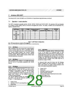
Function Event Mask Register (offset +04 from BAR4)
This register controls the assertion of the device’s interrupt pin and the CSYSCHG pin.
Reserved
15 14 Reserved
4 3 2 1 0
BIt0 - WP (Write Protect).
Not implemented. Returns 0.
Bit1 – Ready.
Not implemented. Returns 0.
Not implemented. Returns 0.
Not implemented. Returns 0.
BIt2 – Battery Voltage Detect 2 (BVD2).
Bit3 – Battery Voltage Detect 1 (BVD1)
Bit4 – General Wakeup (GWAKE)
Bit14 – Wakeup (WKUP)
Set according to the PME_En bit in the PCI power Management Registers.
Default value returns 0 (wakeups disabled)
Set according to the PME_En bit in the PCI power Management Registers
Default value returns 0 (wakeups disabled)
Bits 4, 14 collectively control the assertion of the power management event line
CSYSCHG when an internal wakeup request has been latched into the
GWAKE field in the function event register.
Bit 15 – Interrupt (INTR)
Interrupt Mask. Controls the assertion of the cardbus CINT# line when an
internal interrupt/powerdown request has been latched into the corresponding
field in the Function Event register. Default value is 0 (interrupts disabled)
DS-0033 Sep 05
External-Free Release
Page 25

 OXFORD [ OXFORD SEMICONDUCTOR ]