OXCB950
OXFORD SEMICONDUCTOR LTD.
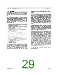
7.2 Register description tables
The UART is accessed through an 8-byte block of I/O space (or through memory space). Since there are more than 8 registers,
the mapping is also dependent on the state of the Line Control Register ‘LCR’ and Additional Control Register ‘ACR’:
1. LCR[7]=1 enables the divider latch registers DLL and DLM.
2. LCR specifies the data format used for both transmitter and receiver. Writing 0xBF (an unused format) to LCR enables
access to the 650 compatible register set. Writing this value will set LCR[7] but leaves LCR[6:0] unchanged. Therefore, the
data format of the transmitter and receiver data is not affected. Write the desired LCR value to exit from this selection.
3. ACR[7]=1 enables access to the 950 specific registers.
4. ACR[6]=1 enables access to the Indexed Control Register set (ICR) registers as described on page 32.
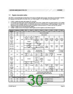
Register Address R/W
Name
Bit 7
Bit 6
Bit 5
Bit 4
Bit 3
Bit 2
Bit 1
Bit 0
1
THR
000
W
Data to be transmitted
Data received
1
RHR
000
R
1,2
IER
CTS
interrupt
mask
RTS
interrupt
mask
Special
Char.
650/950
Mode
Modem
Sleep
Rx Stat
interrupt
mask
THRE
interrupt
mask
RxRDY
interrupt
mask
Detect
001
010
R/W
W
interrupt
mode
Alternate
mask
550/750
Mode
Unused
sleep
mode
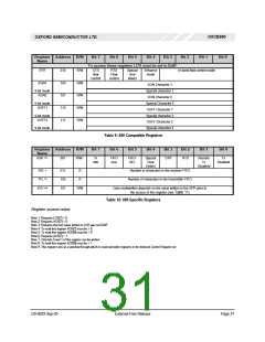
3
FCR
RHR Trigger
Level
THR Trigger
650 mode
750 mode
Level
Tx
Flush
THR
Flush
RHR
Enable
FIFO
RHR Trigger
Level
FIFO
Size
Trigger
Enable
Unused
950 mode
Unused
FIFOs
Interrupt priority
Interrupt priority
(All modes)
Interrupt
pending
3
ISR
010
011
R
enabled
(Enhanced mode)
Divisor
Odd /
Number
of stop
bits
Tx
Force
even
Parity
4
LCR
R/W
latch
Data length
break
parity
enable
access
parity
CTS &
RTS
3,4
MCR
Enable
Internal
Loop
550/750
Mode
Unused
Flow
100
R/W
Unused
RTS
DTR
Control
Back
650/950
Mode
Baud
IrDA
XON-Any
prescale
mode
3,5
LSR
Data
THR
Rx
Framing
Error
Parity
Error
Overrun
Error
Tx Empty
RxRDY
Normal
Error
Empty
Break
101
R
9-bit data
9th Rx
mode
data bit
Delta
DCD
Trailing
Delta
DSR
Delta
CTS
3
MSR
110
111
R
DCD
RI
DSR
CTS
RI edge
3
SPR
Temporary data storage register and
Normal
Indexed control register offset value bits
R/W
9-bit data
9th Tx
Unused
mode
data bit
Additional Standard Registers – These registers require divisor latch access bit (LCR[7]) to be set to 1.
DLL
000
001
R/W
R/W
Divisor latch bits [7:0] (Least significant byte)
Divisor latch bits [15:8] (Most significant byte)
DLM
Table 8: Standard 550 Compatible Registers
External-Free Release
DS-0033 Sep 05
Page 30

 OXFORD [ OXFORD SEMICONDUCTOR ]