OXCB950
OXFORD SEMICONDUCTOR LTD.
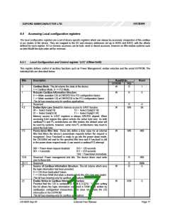
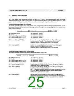
Note1
GIS(22) is the inverse of UMR(16).
Note 2:
The returned value is either the direct state of the corresponding MIO pin or its inverse as configured by the Multi-purpose I/O Configuration register
‘MIC’ (offset 0x04). As the internal MIO can assert a cardbus/PCI interrupt, the inversion feature can define each external interrupt to be defined as
active-low or active-high, as controlled by the MIC register.
Note 3:
The UART Interrupt Enable register bit is set after a hardware reset to enable the interrupt from the internal UART. This will cater for generic device-
driver software that does not access the Local Configuration Registers. The default setting for the UART Interrupt Enable bit can be changed using
the serial EEPROM. Note that even though the UART interrupt is enabled in this register, by default after a reset the IER register of the UART is
disabled so a cardbus/PCI interrupt will not be asserted by the UART after a hardware reset.
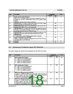
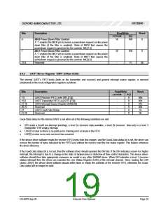
6.5 Cardbus/ PCI Interrupt
Interrupts in cardbus/PCI systems are level-sensitive and
can be shared. In the OXCB950, there are three sources of
interrupts - two from the Multi-Purpose I/O pins (MIO0,
MIO1), and one from the internal UART.
The 3 sources of interrupts on the OXCB950, can be
enabled/disabled individually using the options in the local
configuration register “GIS”.
By default, these options are enabled so that, irrespective
of the device’s application mode (cardbus or pci), the
assertion of the 2 Multi_Purpose I/O pins (MIO0, MIO1)
will, following the initial cardbus/PCI configuration process,
assert the interrupt pin of the device. By the same token,
any UART based interrupts that are generated as a result
of enabling interrupts in the UART’s interrupt register (the
ISR register), will result in the assertion of the UART
interrupt on the interrupt pin of the device.
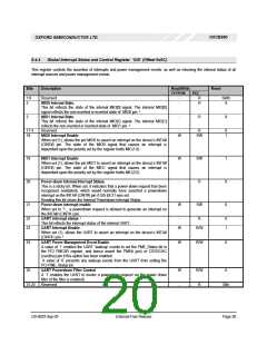
Since the OXCB950 has only one interrupt pin (INTA# /
CINT#), the default routing information contained in the
device (the interrupt pin value) results in all interrupts being
made available on this single interrupt pin.
This default routing may be modified (to disable all
interrupts, for example) by writing to the Interrupt Pin field
in the cardbus/PCI configuration registers using the serial
EEPROM facility. The Interrupt Pin field is normally
considered a hard-wired read-only value in cardbus/PCI. It
indicates to system software which interrupt pin (if any) is
used by a function. The interrupt pin may only be modified
using the serial EEPROM facility, and card developers
must not set any value which violates the cardbus/PCI
specification on this issue. If in doubt, the default routings
should be used. Table 6 relates the Interrupt Pin field to the
device pin used.
Once an interrupt has been asserted, this interrupt can only
be removed by the device driver either by disabling the
relevant controls in the GIS register or by removing the
conditions on the 3 interrupt sources. For the UART, this
will require reads of the relevant register to clear any UART
based interrupts.
Cardbus applications, normally expect a set of four 32-bit
registers: Function Event, Function Event Mask, Function
Present State, and Function Force Event Registers to
control the assertion/deassertion of interrupts (and power
management events). These are the cardbus status
registers located in memory space at the location given by
the CISTPL_CONFIG_CB tuple. For the OXCB950, these
registers reside at the memory base address register BAR4
that is dedicated to provide access to these additional
registers. By default, in cardbus mode, these status
registers are disabled (bypassed) so cardbus applications
exhibit the same interrupt behaviour as per the pci mode.
This default setting is particularly suitable for those
applications, such as Windows 9x, that treat cardbus
functions as PCI functions and continue to utilise (modified)
versions of PCI device drivers for cardbus functionality.
These PCI based device drivers do not expect the
presence of these cardbus status registers to further
control the interrupt generation / deassertion logic.
Interrupt Pin
Device Pin used
None
0
1
INTA# (CINT#)
Reserved
2 to 255
Table 6: ‘Interrupt pin’ definition
During the system initialisation process and cardbus/PCI
device configuration, system-specific software reads the
interrupt pin field to determine which (if any) interrupt pin is
used by the function. It programmes the system interrupt
router to logically connect this interrupt pin to a system-
specific interrupt vector (IRQ). It then writes this routing
information to the Interrupt Line field in the function’s
cardbus/PCI configuration space. Device driver software
must then hook the interrupt using the information in the
Interrupt Line field.
The Interrupt status for all sources of interrupts are
available using the GIS register in the Local Configuration
Register set, which can be accessed using I/O or Memory
accesses.
For those cardbus applications that do require use of these
cardbus status registers, these registers can be enabled by
setting LCC, bit 23 located in the device’s local
configuration registers. This can be achieved by performing
DS-0033 Sep 05
External-Free Release
Page 21

 OXFORD [ OXFORD SEMICONDUCTOR ]