OXCB950
OXFORD SEMICONDUCTOR LTD.
6.4 Accessing Local configuration registers
The local configuration registers are a set of device specific registers which can always be accessed, irrespective of the cardbus
or pci modes of the device. They are mapped to the I/O and memory addresses set up in BAR2 and BAR3, with the offsets
defined for each register. I/O or memory accesses can be byte, word or dword accesses, however on little-endian systems such
as Intel 80x86 the byte order will be reversed.
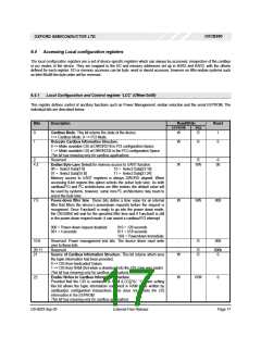
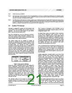
6.4.1 Local Configuration and Control register ‘LCC’ (Offset 0x00)
This register defines control of ancillary functions such as Power Management, endian selection and the serial EEPROM. The
individual bits are described below.
Bits
0
Description
Read/Write
EEPROM
Reset
PCI
Cardbus Mode. This bit returns the state of the device.
1=> Cardbus Mode. 0 => PCI Mode.
W
R
1
0
1
Relocate Cardbus Information Structure.
W
R
0 => Make available CIS at DWORD18 in PCI configuration Space
1 => Make available CIS at DWORD32 in the PCI configuration Space
This bit has meaning only for cardbus applications.
Reserved
2
-
R
0
4:3
Endian Byte-Lane Select for memory access to UART function.
W
RW
00
00 = Select Data[7:0]
01 = Select Data[15:8]
10 = Select Data[23:16]
11 = Select Data[31:24]
Memory access to UART registers is always DWORD aligned. When
accessing 8-bit regions this option selects the active byte lane. As both
cardbus/PCI and PC architectures are little endian, the default value will
be used by systems, however, some non-PC architectures may need to
select the byte lane.
7:5
Power-down filter time. These bits define a time value for an internal
filter that filters the device’s powerdown requests before the request is
recognised. Once Function0 is ready to go into the power down mode,
the OXCB950 will wait for the specified filter time and if Function0 is still
in the power-down request mode, it can assert a cardbus/PCI interrupt
W
RW
000
000 = Power-down request disabled
001 = 4 seconds
010 = 129 seconds
011 = 518 seconds
1XX = Powerdown Immediate
10:8
Reserved: Power management test bits. The device driver must write
zero to these bits
-
R
000
20:11
21
Reserved.
-
R
R
000h
0
Source of Cardbus Information Structure. This bit returns which area
the tuple information had been provided.
W
0 => CIS from hardcoded Values
1 => CIS from RAM (Set when a download into the CIS zone was made)
This bit has meaning only for cardbus applications.
Enable Writes to Cardbus InformationStructure.
Provided that the CIS is contained in RAM (LCC[21]= ‘1’), then setting
this bit allows the tuple information contained in RAM to be written by
cardbus/pci configuration transactions. This does not update the CIS
information in the EEPROM.
22
W
R/W
0
This bit has meaning only for cardbus applications
DS-0033 Sep 05
External-Free Release
Page 17

 OXFORD [ OXFORD SEMICONDUCTOR ]