OXCB950
OXFORD SEMICONDUCTOR LTD.
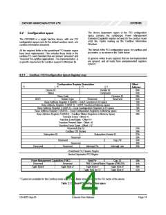
Bits
Description
Read/Write
Reset
EEPROM
PCI
23
Enable Cardbus Status Registers
W
R/W
0
When set (1), all interrupt sources and power management events are
controlled by the INTR, GWAKE/WKUP fields of the cardbus status
registers.
This bit has meaning only for cardbus applications
EEPROM Clock. For reads or writes to the external EEPROM , toggle
this bit to generate an EEPROM clock (EE_CK pin).
EEPROM Chip Select. When 1 the EEPROM chip-select pin EE_CS is
activated (high). When 0 EE_CS is de-active (low).
EEPROM Data Out. For writes to the EEPROM, this output bit feeds the
input-data of the external EEPROM. This bit is output on the devices
EE_DO and clocked into the EEPROM by EE_CK.
EEPROM Data In. For reads from the EEPROM, this input bit is the
output-data (D0) of the external EEPROM connected to EE_DI pin.
EEPROM Valid.
24
25
26
-
-
-
RW
RW
RW
0
0
0
27
28
29
-
-
-
R
R
1
X
0
A 1 indicates that a valid EEPROM program header is present
Reload configuration from EEPROM.
RW
Writing a 1 to this bit re-loads the configuration from EEPROM. This bit is
self-clearing after an EEPROM read
30
31
Reserved
-
-
R
R
0
0
Reserved
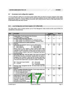
6.4.2 Multi-purpose I/O Configuration register ‘MIC’ (Offset 0x04)
This register configures the operation of the multi-purpose I/O pins ‘MIO[1:0]’ as follows.
Bits
Description
Read/Write
Reset
EEPROM
PCI
RW
1:0
MIO0 Configuration Register
W
00
00 -> MIO0 is a non-inverting input pin
01 -> MIO0 is an inverting input pin
10 -> MIO0 is an output pin driving ‘0’
11 -> MIO0 is an output pin driving ‘1’
3:2
MIO1 Configuration Register
W
RW
00
00 -> MIO1 is a non-inverting input pin
01 -> MIO1 is an inverting input pin
10 -> MIO1 is an output pin driving ‘0’
11 -> MIO1 is an output pin driving ‘1’
4
5
MIO0 Power Management Event Enable.
W
W
RW
RW
0
0
A value of ‘1’ enables the MIO0 pin to set the PME_Status bit in the PCI
PMCSR register, and hence assert the PME# (pci) or CSYSCHG
(cardbus) pin if this option has been enabled.
A value of ‘0’ prevents MIO0 from setting the PCI PME_Status bit.
MIO1 Power Management Event Enable.
A value of ‘1’ enables the MIO1 pin to set the PME_Status bit in the PCI
PMCSR register, and hence assert the PME# (pci) or CSYSCHG
(cardbus) pin if this option has been enabled.
A value of ‘0’ prevents MIO1 from setting the PCI PME_Status bit.
DS-0033 Sep 05
External-Free Release
Page 18

 OXFORD [ OXFORD SEMICONDUCTOR ]