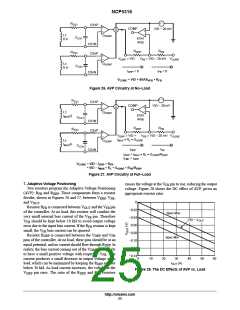
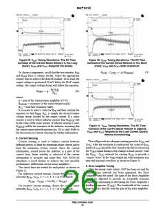
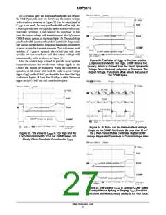
NCP5316
I
is the RMS value of the trapezoidal current in
RMS,CNTL
the control MOSFET:
I
D
Ǹ
(20)
I
+ D
RMS,CNTL
2
2
) I )ń3]
Lo,MIN
1ń2
(21)
(22)
@ [(I
) I
@ I
Lo,MAX
Lo,MAX Lo,MIN
V
GATE
I
I
I
is the maximum output inductor current:
Lo,MAX
I
+ I
O,MAX
ńf ) D I ń2
Lo
Lo,MAX
is the minimum output inductor current:
V
Lo,MIN
O,MAX
GS_TH
I
+ I
O,MAX
ńf * D I ń2
Lo
Lo,MIN
is the maximum converter output current.
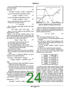
Q
Q
Q
V
DRAIN
GS1
GS2
GD
D is the duty cycle of the converter:
(23)
D + V
ńV
OUT IN
Figure 25. MOSFET Switching Characteristics
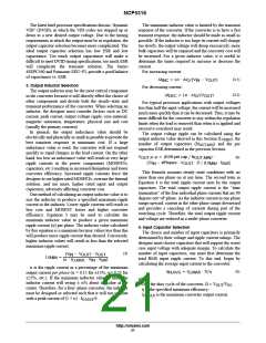
DI is the peak−to−peak ripple current in the output
Lo
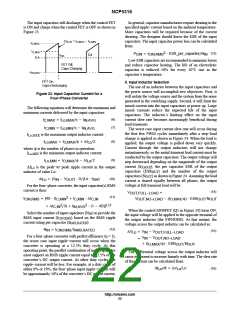
When the MOSFET power dissipations are known, the
designer can calculate the required thermal impedance to
maintain a specified junction temperature at the worst case
ambient operating temperature.
inductor of value L :
o
(24)
D I + (V * V
Lo IN
) @ Dń(Lo @ f )
OUT SW
R
DS(on)
is the ON resistance of the MOSFET at the
applied gate drive voltage.
is the post gate threshold portion of the
(28)
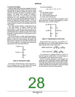
q
T
t (T * T )ńP
J A D
Q
switch
gate−to−sourcecharge plus the gate−to−drain charge. This
may be specified in the data sheet or approximated from the
gate−charge curve as shown in the Figure 25.
(25)
where:
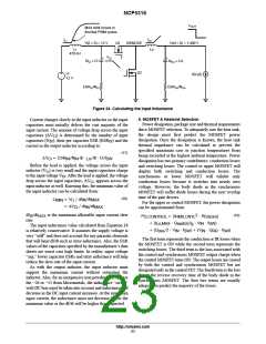
q is the total thermal impedance (q + q );
T
JC
SA
q
is the junction−to−case thermal impedance of the
JC
MOSFET;
is the sink−to−ambient thermal impedance of the
Q
+ Q
) Q
gs2 gd
switch
q
SA
I is the output current from the gate driver IC.
g
heatsink assuming direct mounting of the MOSFET (no
thermal “pad” is used);
V
IN
is the input voltage to the converter.
f
Q
is the switching frequency of the converter.
is the MOSFET total gate charge to obtain R
sw
T
is the specified maximum allowed junction
temperature;
J
;
DS(on)
G
commonly specified in the data sheet.
V is the gate drive voltage.
T is the worst case ambient operating temperature.
A
g
For TO−220 and TO−263 packages, standard FR−4
copper clad circuit boards will have approximate thermal
resistances (q ) as shown below:
Q
Q
is the reverse recovery charge of the lower MOSFET.
is the MOSFET output charge specified in the data
RR
oss
SA
sheet.
For the lower or synchronous MOSFET, the power
dissipation can be approximated from:
Pad Size
Single−Sided
2
2
(in /mm )
0.50/323
0.75/484
1.00/645
1.50/968
1 oz. Copper
60−65°C/W
55−60°C/W
50−55°C/W
45−50°C/W
2
P
+ (I
RMS,SYNCH
@ R
)
DS(on)
D,SYNCH
) (Vf
(26)
@ I
diode O,MAX
ń2 @ t_nonoverlap @ f )
SW
where:
Vf
is the forward voltage of the MOSFET’s intrinsic
diode
diode at the converter output current.
t_nonoverlap is the non−overlap time between the upper
and lower gate drivers to prevent cross conduction.
This time is usually specified in the data sheet for the
control IC.
The first term represents the conduction or IR losses when
the MOSFET is ON and the second term represents the diode
losses that occur during the gate non−overlap time.
All terms were defined in the previous discussion for the
control MOSFET with the exception of:
As with any power design, proper laboratory testing
should be performed to insure the design will dissipate the
required power under worst case operating conditions.
Variables considered during testing should include
maximum ambient temperature, minimum airflow,
maximum input voltage, maximum loading and component
variations (i.e., worst case MOSFET R
). Also, the
DS(on)
inductors and capacitors share the MOSFET’s heatsinks and
will add heat and raise the temperature of the circuit board
and MOSFET. For any new design, it is advisable to have as
much heatsink area as possible. All too often, new designs are
found to be too hot and require re−design to add heatsinking.
Ǹ
(27)
I
+ 1 * D
RMS,SYNCH
2
2 1ń2
) I )ń3]
Lo,MIN
@ [(I
Lo,MAX
) I
@ I
Lo,MAX Lo,MIN
http://onsemi.com
24

 ONSEMI [ ONSEMI ]