NCP5316
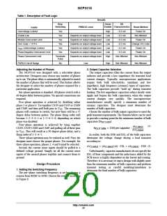
Table 1. Description of Fault Logic
Results
Driver
Stop
Switching
SS
Enable Characteristics
PWRGD Level
Reset Method
Power On
Faults
Overvoltage Lockout
Enable Low
Yes
Yes
Yes
Yes
Yes
Yes
High
Low
Low
Low
Low
Low
High
−0.3 mA
−0.3 mA
Depends on output voltage level
Depends on output voltage level
Depends on output voltage level
Depends on output voltage level
Depends on output voltage level
Depends on output voltage level
Not Affected
Power On
Module Overcurrent Limit
DAC Code = 11111x
−0.3 mA
−0.3 mA
Change VID Code
Power On
V
REF
Undervoltage Lockout
−0.3 mA
Phase Negative Overcurrent Limit
Phase Overcurrent Limit
−0.3 mA
Power On
Terminate
Pulse
Not Affected
Not Affected
PWRLS Out of Range
No
Low
High
Not Affected
Not Affected
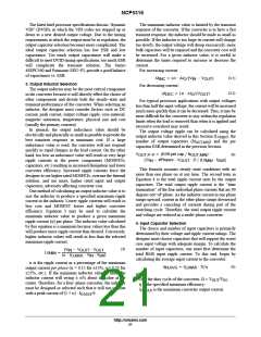
Adjusting the Number of Phases
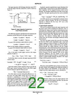
2. Output Capacitor Selection
The NCP5316 was designed with a selectable−phase
architecture. Designers may choose any number of phases
up to six. The phase delay is automatically adjusted to match
the number of phases that will be used. This feature allows
the designer to select the number of phases required for a
particular application.
Six−phase operation is standard. All phases switch with a
60 degree delay between pulses. No special connections are
required.
The output capacitors filter the current from the output
inductor and provide a low impedance for transient load
current changes. Typically, microprocessor applications
require both bulk (electrolytic, tantalum) and low
impedance, high frequency (ceramic) types of capacitors.
The bulk capacitors provide “hold up” during transient
loading. The low impedance capacitors reduce steady−state
ripple and bypass the bulk capacitance when the output
current changes very quickly. The microprocessor
manufacturers usually specify a minimum number of
ceramic capacitors. The designer must determine the
number of bulk capacitors.
Five−phase operation is achieved by disabling either
phase 3 or phase 6. Tie together CS3N and CS3P or CS6N
and CS6P, and then pull both pins to V . The remaining
CC
phases will continue to switch, but now there will be a 72
degree delay between pulses. The phase firing order will
become 1−2−3−4−5 or 1−2−4−5−6, depending on which
phase was disabled.
Choose the number of bulk output capacitors to meet the
peak transient requirements. The formula below can be used
to provide a starting point for the minimum number of bulk
capacitors (N
):
OUT,MIN
Four−phase operation is achieved by tying together
CS3N, CS3P, CS6N and CS6P, and pulling all of these pins
(1)
D I
O,MAX
N
+ ESR per capacitor @
OUT,MIN
D V
O,MAX
to V . This will result in a 90 degree phase delay, and a
CC
firing order of 1−2−4−5.
In reality, both the ESR and ESL of the bulk capacitors
determine the voltage change during a load transient
according to:
Three−phase operation may be realized as well. First, the
designer must choose the proper phases. For example, for
three−phase operation, phases 2, 4 and 6 must be selected.
Second, the current sense inputs should be pulled to a
defined voltage ground. Simply tie all the current sense
inputs of the unused phases together and connect them to
ground.
(2)
ńD t) @ ESL ) D I @ ESR
O,MAX
D V
+ (D I
O,MAX
O,MAX
Unfortunately, capacitor manufacturers do not specify the
ESL of their components and the inductance added by the
PCB traces is highly dependent on the layout and routing.
Therefore, it is necessary to start a design with slightly more
than the minimum number of bulk capacitors and perform
transient testing or careful modeling/simulation to
determine the final number of bulk capacitors.
Design Procedure
1. Setting the Switching Frequency
The per−phase switching frequency is set by placing a
resistor from ROSC to GND. Choose the resistor according
to Figure 6.
http://onsemi.com
20

 ONSEMI [ ONSEMI ]