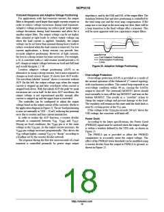
NCP5316
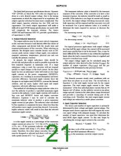
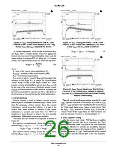
The input capacitors will discharge when the control FET
is ON and charge when the control FET is OFF as shown in
Figure 23.
In general, capacitor manufacturers require derating to the
specified ripple−current based on the ambient temperature.
More capacitors will be required because of the current
derating. The designer should know the ESR of the input
capacitors. The input capacitor power loss can be calculated
from:
D I
C,IN
= I
− I
C,MAX C,MIN
I
C,MAX
I
C,MIN
2
+ I @ ESR_per_capacitorńN
CIN,RMS IN
(13)
P
CIN
t
T/4
ON
0 A
Low ESR capacitors are recommended to minimize losses
and reduce capacitor heating. The life of an electrolytic
capacitor is reduced 50% for every 10°C rise in the
capacitor’s temperature.
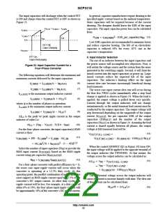
FET Off,
Caps Charging
−I
IN,AVG
FET On,
Caps Discharging
5. Input Inductor Selection
The use of an inductor between the input capacitors and
the power source will accomplish two objectives. First, it
will isolate the voltage source and the system from the noise
generated in the switching supply. Second, it will limit the
inrush current into the input capacitors at power up. Large
inrush currents reduce the expected life of the input
capacitors. The inductor’s limiting effect on the input
current slew rate becomes increasingly beneficial during
load transients.
The worst case input current slew rate will occur during
the first few PWM cycles immediately after a step−load
change is applied as shown in Figure 24. When the load is
applied, the output voltage is pulled down very quickly.
Current through the output inductors will not change
instantaneously, so the initial transient load current must be
conducted by the output capacitors. The output voltage will
step downward depending on the magnitude of the output
Figure 23. Input Capacitor Current for a
Four−Phase Converter
The following equations will determine the maximum and
minimum currents delivered by the input capacitors:
(6)
(7)
I
+ I
ńh * I
C,MAX
Lo,MAX
ńh * I
Lo,MIN
IN,AVG
I
+ I
C,MIN
IN,AVG
I
is the maximum output inductor current:
Lo,MAX
(8)
(9)
I
+ I
O,MAX
ńf ) D I ń2
Lo
Lo,MAX
where f is the number of phases in operation.
is the minimum output inductor current:
I
Lo,MIN
I
+ I
O,MAX
ńf * D I ń2
Lo
Lo,MIN
current (I
), the per capacitor ESR of the output
DI is the peak−to−peak ripple current in the output
O,MAX
Lo
capacitors (ESR
) and the number of the output
OUT
inductor of value Lo:
capacitors (N
) as shown in Figure 24. Assuming the load
OUT
(10)
D I + (V * V
Lo IN
) @ Dń(Lo @ f )
OUT SW
current is shared equally between all phases, the output
voltage at full transient load will be:
For the four−phase converter, the input capacitor(s) RMS
current is then:
(14)
V
+
OUT,FULL−LOAD
V
(11)
2
I
+ [4D @ (I
C,MIN
) I @ D I
C,MIN C,IN
* (I
O,MAX
ńf ) @ ESR
ńN
OUT OUT
CIN,RMS
OUT,NO−LOAD
2
2
1ń2
@ (1 * 4D)]
) D I
C,IN
ń3) ) I
IN,AVG
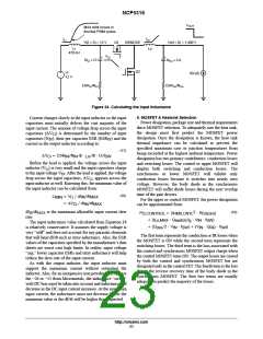
When the control MOSFET (Q1 in Figure 24) turns ON,
the input voltage will be applied to the opposite terminal of
the output inductor (the SWNODE). At that instant, the
voltage across the output inductor can be calculated as:
Select the number of input capacitors (N ) to provide the
IN
RMS input current (I
) based on the RMS ripple
CIN,RMS
current rating per capacitor (I
):
RMS,RATED
(12)
N
+ I
ńI
IN
CIN,RMS RMS,RATED
(15)
D V + V * V
Lo
IN
OUT,FULL−LOAD
OUT,NO−LOAD
For a four−phase converter with perfect efficiency (h = 1),
the worst case input ripple−current will occur when the
converter is operating at a 12.5% duty cycle. At this
operating point, the parallel combination of input capacitors
must support an RMS ripple current equal to 12.5% of the
converter’s DC output current. At other duty cycles, the
ripple−current will be less. For example, at a duty cycle of
either 6% or 19%, the four−phase input ripple−current will
be approximately 10% of the converter’s DC output current.
V
* V
+
IN
) (I
ńf ) @ ESR
ńN
OUT OUT
O,MAX
The differential voltage across the output inductor will
cause its current to increase linearly with time. The slew rate
of this current can be calculated from:
dI ńdt + D V ńLo
Lo Lo
(16)
http://onsemi.com
22

 ONSEMI [ ONSEMI ]