NCP5316
SWNODE
Q2
V
OUT
MAX dI/dt occurs in
first few PWM cycles.
I
I
Lo
Li
Vi(t = 0) = 12 V
Q1
Vo(t = 0) = 1.480 V
Li
Lo
470 nH
V
Ci
+
+
N
× Ci
N
× Co
Ci
Co
Vi
12 V
+
−
60 u(t)
ESR /N
ESR /N
Co Co
Ci Ci
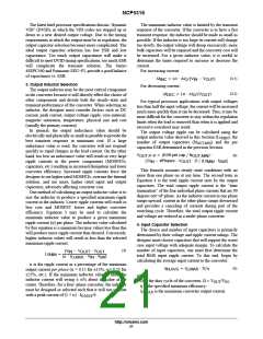
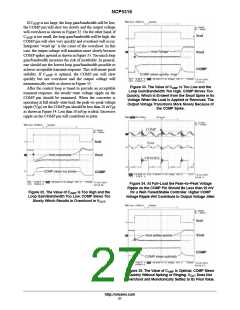
Figure 24. Calculating the Input Inductance
6. MOSFET & Heatsink Selection
Current changes slowly in the input inductor so the input
capacitors must initially deliver the vast majority of the
input current. The amount of voltage drop across the input
Power dissipation, package size and thermal requirements
drive MOSFET selection. To adequately size the heat sink,
the design must first predict the MOSFET power
dissipation. Once the dissipation is known, the heat sink
thermal impedance can be calculated to prevent the
specified maximum case or junction temperatures from
being exceeded at the highest ambient temperature. Power
dissipation has two primary contributors: conduction losses
and switching losses. The control or upper MOSFET will
display both switching and conduction losses. The
synchronous or lower MOSFET will exhibit only
conduction losses because it switches into nearly zero
voltage. However, the body diode in the synchronous
MOSFET will suffer diode losses during the non−overlap
time of the gate drivers.
capacitors (DV ) is determined by the number of input
Ci
capacitors (N ), their per capacitor ESR (ESR ) and the
IN
IN
current in the output inductor according to:
(17)
D V + ESR ńN dl @ ńdt @ Dńf
Ci IN IN Lo
SW
Before the load is applied, the voltage across the input
inductor (V ) is very small and the input capacitors charge
Li
to the input voltage V . After the load is applied, the voltage
IN
drop across the input capacitors, DV , appears across the
Ci
input inductor as well. Knowing this, the minimum value of
the input inductor can be calculated from:
(18)
+ V ń dI ńdt
Li IN MAX
Li
MIN
For the upper or control MOSFET, the power dissipation
can be approximated from:
+ D V ń dI ńdt
Ci IN MAX
dI /dt
rate.
is the maximum allowable input current slew
(19)
2
IN MAX
P
+ (I
@ R
)
DS(on)
D,CONTROL
RMS,CNTL
@ Q ńI @ V @ f
) (I
)
Lo,MAX
switch g IN SW
The input inductance value calculated from Equation 18
is relatively conservative. It assumes the supply voltage is
very “stiff” and does not account for any parasitic elements
that will limit dI/dt such as stray inductance. Also, the ESR
values of the capacitors specified by the manufacturer’s data
sheets are worst case high limits. In reality, input voltage
“sag,” lower capacitor ESRs and stray inductance will help
reduce the slew rate of the input current.
As with the output inductor, the input inductor must
support the maximum current without saturating the
inductor. Also, for an inexpensive iron powder core, such as
the −26 or −52 from Micrometals, the inductance “swing”
with DC bias must be taken into account and inductance will
decrease as the DC input current increases. At the maximum
input current, the inductance must not decrease below the
minimum value or the dI/dt will be higher than expected.
) (Q
ń2 @ V @ f
) ) (V @ Q
IN SW IN
@ f )
RR SW
oss
The first term represents the conduction or IR losses when
the MOSFET is ON while the second term represents the
switching losses. The third term is the loss associated with
the control and synchronous MOSFET output charge when
the control MOSFET turns ON. The output losses are caused
by both the control and synchronous MOSFET but are
dissipated only in the control FET. The fourth term is the loss
due to the reverse recovery time of the body diode in the
synchronous MOSFET. The first two terms are usually
adequate to predict the majority of the losses.
http://onsemi.com
23

 ONSEMI [ ONSEMI ]