NCP5316
+ −
R
R
CS1
CS1P
+
−
G
+
−
COMP
VID − 20 mV
S
L1
0 A
VDRP
C
CS1
Error
Amp
CS1N
CSxP
R
R
FB
DRP
CSx
+
−
V
DRP
= VID
V
FB
= VID − 20 mV
V
CORE
Lx
0 A
G
VDRP
C
CSx
I
= 0
I
FB
= 0
DRP
CSxN
V
CORE
= VID + IBIAS
w R
VFB
FB
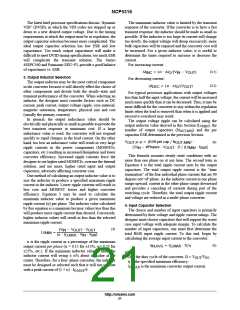
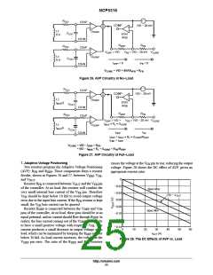
Figure 26. AVP Circuitry at No−Load
+ −
VID − 20 mV
R
CS1
CS1P
+
+
−
COMP
S
−
G
L1
VDRP
Error
Amp
I
/2
MAX
C
CS1
CS1N
CSxP
R
R
FB
DRP
R
CSx
+
−
V
I
= VID +
V
= VID − 20 mV V
CORE
DRP
MAX
FB
• R • G
L
VDRP
Lx
G
VDRP
I
/n
MAX
C
CSx
I
I
FB
CSxN
DRP
I
I
= I
= I
• R • G /R
VDRP DRP
DRP
FBK
MAX
DRP
L
V
CORE
= VID − I
= VID − I
w R
FB
DRP
w R w G
w R /R
FB DRP
MAX
L
VDRP
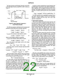
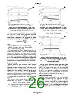
Figure 27. AVP Circuitry at Full−Load
7. Adaptive Voltage Positioning
causes the voltage at the V pin to rise, reducing the output
FB
Two resistors program the Adaptive Voltage Positioning
(AVP): R and R . These components form a resistor
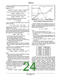
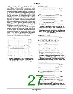
voltage. Figure 28 shows the DC effect of AVP, given an
appropriate resistor ratio.
FB
DRP
divider, shown in Figures 26 and 27, between V , V
,
DRP FB
0
and V
.
OUT
Resistor R is connected between V
of the controller. At no load, this resistor will conduct the
very small internal bias current of the V pin. Therefore
and the V pin
FB
FB
OUT
−0.02
Spec Max
FB
−0.04
VID − V
OUT
V
FB
should be kept below 10 kW to avoid output voltage
−0.06
−0.08
−0.10
−0.12
−0.14
error due to the input bias current. If the R resistor is kept
FB
small, the V bias current can be ignored.
FB
Resistor R
is connected between the V and V
DRP FB
DRP
Spec Min
pins of the controller. At no load, these pins should be at an
equal potential, and no current should flow through R . In
DRP
reality, the bias current coming out of the V
pin is likely
DRP
to have a small positive voltage with respect to V . This
FB
0
10
20
30
(A)
40
50
60
current produces a small decrease in output voltage at no
I
load, which can be minimized by keeping the R
resistor
OUT
DRP
below 30 kW. As load current increases, the voltage at the
pin rises. The ratio of the R and R resistors
Figure 28. The DC Effects of AVP vs. Load
V
DRP
DRP
FB
http://onsemi.com
25

 ONSEMI [ ONSEMI ]