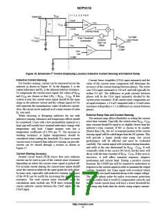
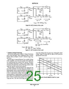
NCP5316
The latest Intel processor specifications discuss “dynamic
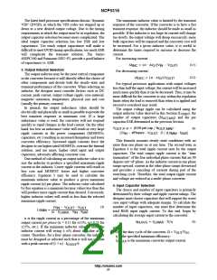
The maximum inductor value is limited by the transient
response of the converter. If the converter is to have a fast
transient response, the inductor should be made as small as
possible. If the inductor is too large its current will change
too slowly, the output voltage will droop excessively, more
bulk capacitors will be required and the converter cost will
be increased. For a given inductor value, it is useful to
determine the times required to increase or decrease the
current.
VID” (DVID), in which the VID codes are stepped up or
down to a new desired output voltage. Due to the timing
requirements at which the output must be in regulation, the
output capacitor selection becomes more complicated. The
ideal output capacitor selection has low ESR and low
capacitance. Too much output capacitance will make it
difficult to meet DVID timing specifications; too much ESR
will complicate the transient solution. The Sanyo
4SEPC560 and Panasonic EEU−FL provide a good balance
of capacitance vs. ESR.
For increasing current:
(3.1)
D t
INC
+ Lo @ D I ń(V * V
IN
)
OUT
O
3. Output Inductor Selection
For decreasing current:
The output inductor may be the most critical component
in the converter because it will directly effect the choice of
other components and dictate both the steady−state and
transient performance of the converter. When selecting an
inductor, the designer must consider factors such as DC
current, peak current, output voltage ripple, core material,
magnetic saturation, temperature, physical size and cost
(usually the primary concern).
(3.2)
D t
DEC
+ Lo @ D I ń(V
)
OUT
O
For typical processor applications with output voltages
less than half the input voltage, the current will be increased
much more quickly than it can be decreased. Thus, it may be
more difficult for the converter to stay within the regulation
limits when the load is removed than when it is applied and
excessive overshoot may result.
In general, the output inductance value should be
electrically and physically as small as possible to provide the
best transient response at minimum cost. If a large
inductance value is used, the converter will not respond
quickly to rapid changes in the load current. On the other
hand, too low an inductance value will result in very large
ripple currents in the power components (MOSFETs,
capacitors, etc.) resulting in increased dissipation and lower
converter efficiency. Increased ripple currents force the
designer to use higher rated MOSFETs, oversize the thermal
solution, and use more, higher rated input and output
capacitors, adversely affecting converter cost.
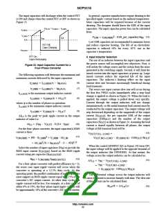
One method of calculating an output inductor value is to
size the inductor to produce a specified maximum ripple
current in the inductor. Lower ripple currents will result in
less core and MOSFET losses and higher converter
efficiency. Equation 3 may be used to calculate the
minimum inductor value to produce a given maximum
ripple current (a ) per phase. The inductor value calculated
by this equation is a minimum because values less than this
will produce more ripple current than desired. Conversely,
higher inductor values will result in less than the selected
maximum ripple current.
The output voltage ripple can be calculated using the
output inductor value derived in this Section (Lo
), the
MIN
number of output capacitors (N ) and the per
OUT,MIN
capacitor ESR determined in the previous Section:
V
+ (ESR per cap ń N
) @
OUT,MIN
(4)
OUT,P−P
NJ
Nj
)
OUT MIN SW
(V * #Phases @ V
IN
) @ D ń (Lo
@ f
This formula assumes steady−state conditions with no
more than one phase on at any time. The second term in
Equation 4 is the total ripple current seen by the output
capacitors. The total output ripple current is the “time
summation” of the four individual phase currents that are 90
degrees out−of−phase. As the inductor current in one phase
ramps upward, current in the other phase ramps downward
and provides a canceling of currents during part of the
switching cycle. Therefore, the total output ripple current
and voltage are reduced in a multi−phase converter.
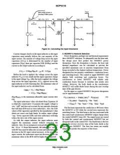
4. Input Capacitor Selection
The choice and number of input capacitors is primarily
determined by their voltage and ripple current ratings. The
designer must choose capacitors that will support the worst
case input voltage with adequate margin. To calculate the
number of input capacitors, one must first determine the
total RMS input ripple current. To this end, begin by
calculating the average input current to the converter:
(3)
(V * V
IN
(a @ I
O,MAX
) @ V
OUT
@ V @ f )
IN SW
OUT
Lo
MIN
+
a is the ripple current as a percentage of the maximum
output current per phase (a = 0.15 for ±15%, a = 0.25 for
±25%, etc.). If the minimum inductor value is used, the
inductor current will swing ± a % about its value at the
center. Therefore, for a four−phase converter, the inductor
must be designed or selected such that it will not saturate
(5)
I
+ I @ Dńh
O,MAX
IN,AVG
where:
D is the duty cycle of the converter, D = V
h is the specified minimum efficiency;
/V ;
OUT IN
I
is the maximum converter output current.
O,MAX
with a peak current of (1 + a ) I
/4.
O,MAX
http://onsemi.com
21

 ONSEMI [ ONSEMI ]