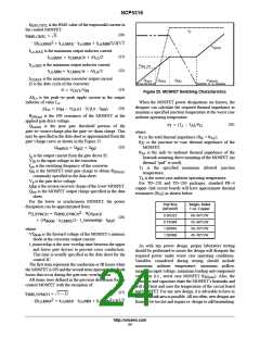
NCP5316
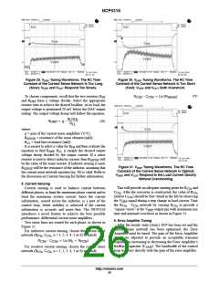
Figure 29. VDRP Tuning Waveforms. The RC Time
Constant of the Current Sense Network Is Too Long
(Slow): VDRP and VOUT Respond Too Slowly.
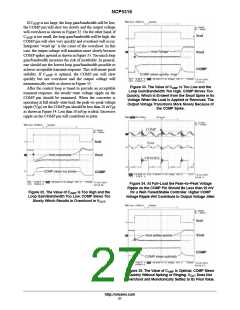
Figure 30. VDRP Tuning Waveforms. The RC Time
Constant of the Current Sense Network Is Too Short
(Fast): VDRP and VOUT Both Overshoot.
(31)
R
@ C
+ Loń(R
)
sense
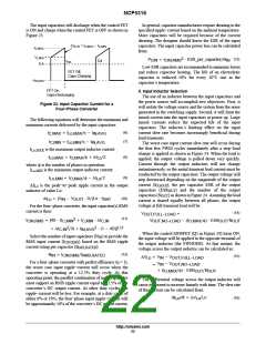
To choose components, recall that the two resistors R
FB
CSx
CSx
and R
form a voltage divider. Select the appropriate
DRP
resistor ratio to achieve the desired loadline. At no load, the
output voltage is positioned 20 mV below the DAC output
setting. The output voltage droop will follow the equation:
R R
L FB
(29)
R
+ g @
DRP
R
LL
where:
g = gain of the current sense amplifiers (V/V);
R
R
= resistance of the sense element (mW);
= load line resistance (mW).
SENSE
LL
It is easiest to select a value for R and then evaluate the
FB
equation to find R . R is simply the desired output
DRP LL
voltage droop divided by the output current. If a sense
resistor is used to detect inductor current, then R
will
SENSE
be the value of the sense resistor. If inductor sensing is used,
will be the resistance of the inductor, assuming that
the current sense network equation (eq. 30) is valid. Refer to
the discussion on Current Sensing for further information.
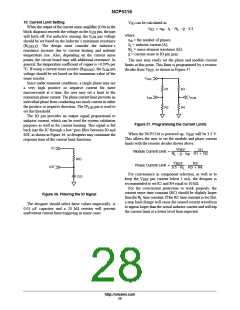
Figure 31. VDRP Tuning Waveforms. The RC Time
Constant of the Current Sense Network Is Optimal:
R
SENSE
V
DRP and VOUT Respond to the Load Current Quickly
Without Overshooting.
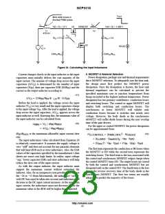
8. Current Sensing
This will provide an adequate starting point for R
and
Current sensing is used to balance current between
different phases, to limit the maximum phase current and to
limit the maximum system current. Since the current
information, sensed across the inductor, is a part of the
control loop, better stability is achieved if the current
information is accurate and noise−free. The NCP5316
introduces a novel feature to achieve the best possible
performance: differential current sense amplifiers.
Two sense lines are routed for each phase, as shown in
Figure 27.
CSx
C
. After the converter is constructed, the value of R
CSx
CSx
(and/or C ) should be fine−tuned in the lab by observing
CSx
the V
signal during a step change in load current. Tune
DRP
the R
C
CSx
network by varying R
to provide a
CSx
CSx
“square−wave” at the V
output pin with maximum rise
DRP
time and minimal overshoot as shown in Figure 31.
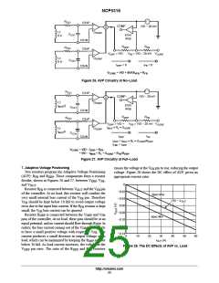
9. Error Amplifier Tuning
After the steady−state (static) AVP has been set and the
current sense network has been optimized, the Error
Amplifier must be tuned. The gain of the Error Amplifier
should be adjusted to provide an acceptable transient
response by increasing or decreasing the Error Amplifier’s
For inductive current sensing, choose the current sense
network (R , C , x = 1, 2, 3, 4, 5 or 6) to satisfy
CSx CSx
(30)
R
@ C
+ Loń(R ) R
)
PCB
CSx
CSx
L
feedback capacitor (C
loop will vary directly with the gain of the error amplifier.
). The bandwidth of the control
For resistive current sensing, choose the current sense
network (R , C , x = 1, 2, 3, 4, 5 or 6) to satisfy
AMP
CSx CSx
http://onsemi.com
26

 ONSEMI [ ONSEMI ]