NCP5316
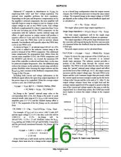
PWRGD
HIGH
V
OUT
PWRGD
low
PWRGD
high
PWRGD
low
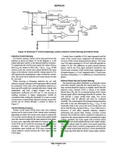
R1
R2
PWRLS
LOW
V
OUT
−2.6% +2.6%
−5.0% +5.0%
VID + 80 mV
V
LOWER
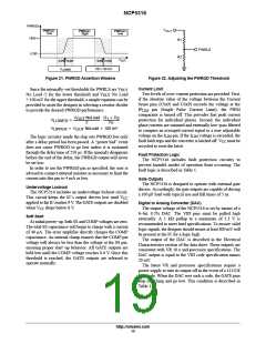
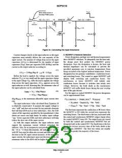
Figure 21. PWRGD Assertion Window
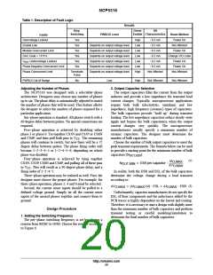
Figure 22. Adjusting the PWRGD Threshold
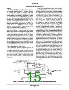
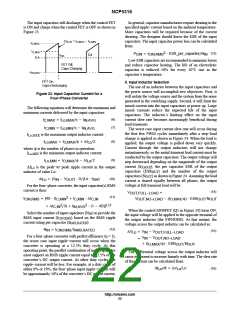
Current Limit
Since the internally−set thresholds for PWRLS are V
OUT
Two levels of over−current protection are provided. First,
if the absolute value of the voltage between the Current
Sense pins (CSxN and CSxP) exceeds the voltage at the
No Load /2 for the lower threshold and V
No Load
OUT
+ 100 mV for the upper threshold, a simple equation can be
provided to assist the designer in selecting a resistor divider
to provide the desired PWRGD performance.
IP
pin (Single Pulse Current Limit), the PWM
LIM
comparator is turned off. This provides fast peak current
protection for individual phases. Second, the individual
phase currents are summed and externally low−pass filtered
to compare an averaged current signal to a user adjustable
V
NoLoad
2
R ) R
OUT
1
2
V
V
+
@
LOWER
UPPER
R
1
+ V
NoLoad ) 100 mV
OUT
voltage on the I
fault latch trips and the converter is latched off. V must be
recycled to reset the latch.
pin. If the I
voltage is exceeded, the
LIM
LIM
The logic circuitry inside the chip sets PWRGD low only
after a delay period has been passed. A “power bad” event
does not cause PWRGD to go low unless it is sustained
through the delay time of 250 m s. If the anomaly disappears
before the end of the delay, the PWRGD output will never
be set low.
In order to use the PWRGD pin as specified, the user is
advised to connect external resistors as necessary to limit the
current into this pin to 4 mA or less.
CC
Fault Protection Logic
The NCP5316 includes fault protection circuitry to
prevent harmful modes of operation from occurring. The
fault logic is described in Table 1.
Gate Outputs
The NCP5316 is designed to operate with external gate
drivers. Accordingly, the gate outputs are capable of driving
a 100 pF load with typical rise and fall times of 5 ns.
Undervoltage Lockout
The NCP5316 includes an undervoltage lockout circuit.
This circuit keeps the IC’s output drivers low until V
CC
applied to the IC reaches 9 V. The GATE outputs are disabled
Digital to Analog Converter (DAC)
when V drops below 8 V.
The output voltage of the NCP5316 is set by means of a
6−bit, 0.5% DAC. The VID pins must be pulled high
externally. A 1 kW pullup to a maximum of 3.3 V is
recommended to meet Intel specifications. To ensure valid
logic signals, the designer should ensure at least 800 mV will
be present at the IC for a logic high.
The output of the DAC is described in the Electrical
Characteristics section of the data sheet. These outputs are
consistent with VR 10.x and processor specifications. The
DAC output is equal to the VID code specification minus
20 mV.
The latest VR and processor specifications require a
power supply to turn its output off in the event of a 11111X
VID code. When the DAC sees such a code, the GATE pins
stop switching and go low. This condition is described in
Table 1.
CC
Soft Start
At initial power−up, both SS and COMP voltages are zero.
The total SS capacitance will begin to charge with a current
of 40 m A. The error amplifier directly charges the COMP
capacitance. An internal clamp ensures that the COMP pin
voltage will always be less than the voltage at the SS pin,
ensuring proper start−up behavior. All GATE outputs are
held low until the COMP voltage reaches 0.6 V. Once this
threshold is reached, the GATE outputs are released to
operate normally.
http://onsemi.com
19

 ONSEMI [ ONSEMI ]