NCP5316
Transient Response and Adaptive Voltage Positioning
impedance, and by the ESR and ESL of the output filter. The
transition between fast and slow positioning is controlled by
the total ramp size and the error amp compensation. If the
ramp size is too large or the error amp too slow, there will be
a long transition to the final voltage after a transient. This
will be most apparent with low capacitance output filters.
For applications with fast transient currents, the output
filter is frequently sized larger than ripple currents require in
order to reduce voltage excursions during load transients.
Adaptive voltage positioning can reduce peak−peak output
voltage deviations during load transients and allow for a
smaller output filter. The output voltage can be set higher
than nominal at light loads to reduce output voltage sag
when the load current is applied. Similarly, the output
voltage can be set lower than nominal during heavy loads to
reduce overshoot when the load current is removed. For low
current applications, a droop resistor can provide fast,
accurate adaptive positioning. However, at high currents,
the loss in a droop resistor becomes excessive. For example,
a 50 A converter with a 1 mW resistor would provide a 50
mV change in output voltage between no load and full load
and would dissipate 2.5 W.
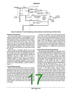
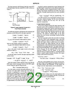
Normal
Fast Adaptive Positioning
SlowAdaptive Positioning
Limits
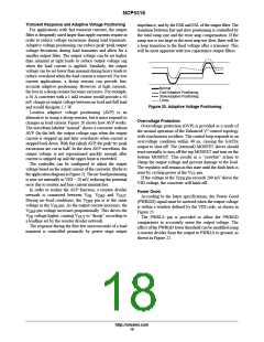
Figure 20. Adaptive Voltage Positioning
Lossless adaptive voltage positioning (AVP) is an
alternative to using a droop resistor, but it must respond to
changes in load current. Figure 20 shows how AVP works.
The waveform labeled “normal” shows a converter without
AVP. On the left, the output voltage sags when the output
current is stepped up and later overshoots when current is
stepped back down. With fast (ideal) AVP, the peak−to−peak
excursions are cut in half. In the slow AVP waveform, the
output voltage is not repositioned quickly enough after
current is stepped up and the upper limit is exceeded.
The controller can be configured to adjust the output
voltage based on the output current of the converter. (Refer to
the application diagram in Figure 2). The no−load positioning
is now set internally to VID − 20 mV, reducing the potential
error due to resistor and bias current mismatches.
Overvoltage Protection
Overvoltage protection (OVP) is provided as a result of
the normal operation of the Enhanced V control topology
with synchronous rectifiers. The control loop responds to an
overvoltage condition within 40 ns, causing the GATEx
output to shut off. The (external) MOSFET driver should
react normally to turn off the top MOSFET and turn on the
bottom MOSFET. This results in a “crowbar” action to
clamp the output voltage and prevent damage to the load.
The regulator will remain in this state until the fault latch is
2
reset by cycling power at the V pin.
CC
If the voltage at the V
pin exceeds 200 mV above the
FFB
VID voltage, the converter will latch off.
In order to realize the AVP function, a resistor divider
Power Good
network is connected between V , V
and V
.
FB
DRP
OUT
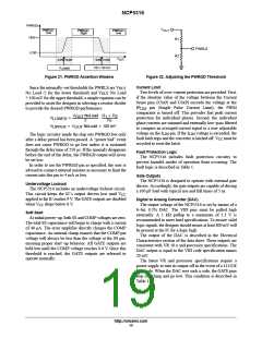
According to the latest specifications, the Power Good
(PWRGD) signal must be asserted when the output voltage
is within a window defined by the VID code, as shown in
Figure 21.
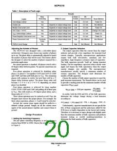
The PWRLS pin is provided to allow the PWRGD
comparators to accurately sense the output voltage. The
effect of the PWRGD lower threshold can be modified using
a resistor divider from the output to PWRLS to ground, as
shown in Figure 22.
During no−load conditions, the V
pin is at the same
DRP
voltage as the V pin. As the output current increases, the
FB
V
V
pin voltage increases proportionally. This drives the
DRP
voltage higher, causing V
to “droop” according to
FB
OUT
a loadline set by the resistor divider network.
The response during the first few microseconds of a load
transient is controlled primarily by power stage output
http://onsemi.com
18

 ONSEMI [ ONSEMI ]