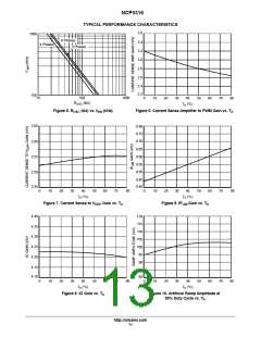
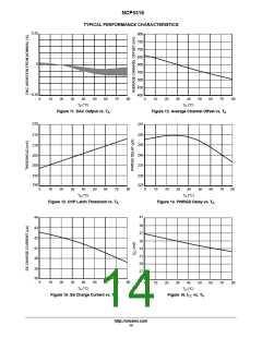
NCP5316
x = 1, 2, 3, 4, 5 or 6
R
CSx
SWNODE
CSxP
+
COx
Lx
C
CSA
CSx
−
CSxN
Internal Ramp
RLx
V
FFB
To PWM
Latch Reset
V
“Fast−Feedback”
OUT
+
−
Channel
Start−Up
Offset
(V
)
Connection
−
CORE
+
V
FB
PWM
COMP
E.A.
+
DAC
Out
COMP
+
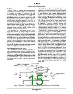
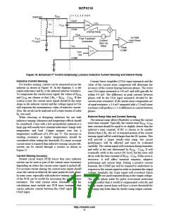
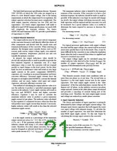
Figure 19. Enhanced V2 Control Employing Lossless Inductive Current Sensing and Internal Ramp
Inductive Current Sensing
For lossless sensing, current can be measured across the
inductor as shown in Figure 19. In the diagram, L is the
Current Sense Amplifier (CSA) input mismatch and the
value of the current sense component will determine the
accuracy of the current sharing between phases. The worst
case CSA input mismatch is ±10 mV and will typically be
within 4.0 mV. The difference in peak currents between
phases will be the CSA input mismatch divided by the
current sense resistance. If all current sense components are
of equal resistance, a 3.0 mV mismatch with a 2.0 mW sense
resistance will produce a 1.5 A difference in current between
phases.
output inductance and R is the inherent inductor resistance.
L
To compensate the current sense signal, the values of R
CSx
. If this
and C
are chosen so that L/R = R
C
CSx
CSx
L
CSx
criteria is met, the current sense signal should be the same
shape as the inductor current and the voltage signal at CSx
will represent the instantaneous value of inductor current.
Also, the circuit can be analyzed as if a sense resistor of value
R was used.
L
External Ramp Size and Current Sensing
The internal ramp allows flexibility in setting the current
sense time constant. Typically, the current sense R
time constant should be equal to or slightly slower than the
inductor’s time constant. If RC is chosen to be smaller
When choosing or designing inductors for use with
inductive sensing, tolerances and temperature effects should
be considered. Cores with a low permeability material or a
large gap will usually have minimal inductance change with
temperature and load. Copper magnet wire has a
temperature coefficient of 0.39% per °C. The increase in
winding resistance at higher temperatures should be
considered when setting the threshold. If a more accurate
current sense is required than inductive sensing can provide,
current can be sensed through a resistor as shown in
Figure 17.
C
CSx
CSx
(faster) than L/R , the AC or transient portion of the current
L
sensing signal will be scaled larger than the DC portion. This
will provide a larger steady−state ramp, but circuit
performance will be affected and must be evaluated
carefully. The current signal will overshoot during transients
and settle at the rate determined by R
C
. It will
CSx
CSx
eventually settle to the correct DC level, but the error will
decay with the time constant of R . If this error is
Current Sharing Accuracy
C
CSx
CSx
Printed circuit board (PCB) traces that carry inductor
current can be used as part of the current sense resistance
depending on where the current sense signal is picked off.
For accurate current sharing, the current sense inputs should
sense the current at relatively the same points for each phase.
In some cases, especially with inductive sensing, resistance
of the PCB can be useful for increasing the current sense
resistance. The total current sense resistance used for
calculations must include any PCB trace resistance that
carries inductor current between the CSxP input and the
CSxN input.
excessive, it will affect transient response, adaptive
positioning and current limit. During a positive current
transient, the COMP pin will be required to undershoot in
response to the current signal in order to maintain the output
voltage. Similarly, the V
signal will overshoot which
DRP
will produce too much transient droop in the output voltage.
The single−phase pulse−by−pulse overcurrent protection
will trip earlier than it would if compensated correctly and
hiccup−mode current limit will have a lower threshold for
fast rising step loads than for slowly rising output currents.
http://onsemi.com
17

 ONSEMI [ ONSEMI ]