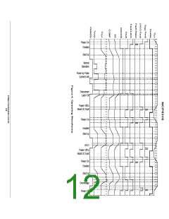
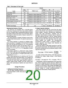
NCP5316
2
Enhanced V responds to disturbances in V
by
or, in a closed loop configuration when the output current
CORE
employing both “slow” and “fast” voltage regulation. The
internal error amplifier performs the slow regulation.
Depending on the gain and frequency compensation set by
the amplifier’s external components, the error amplifier will
typically begin to ramp its output to react to changes in the
output voltage in one or two PWM cycles. Fast voltage
feedback is implemented by a direct connection from Vcore
to the non−inverting pin of the PWM comparator via the
summation with the inductor current, internal ramp and
offset. A rapid increase in output current will produce a
negative offset at Vcore and at the output of the summer.
This will cause the PWM duty cycle to increase almost
instantly. Fast feedback will typically adjust the PWM duty
cycle in one PWM cycle.
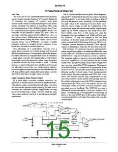
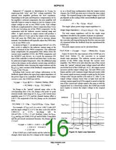
As shown in Figure 17, an internal ramp (100 mV at a 50%
duty cycle) is added to the inductor current ramp at the
positive terminal of the PWM comparator. This additional
ramp compensates for propagation time delays from the
current sense amplifier (CSA), the PWM comparator and
the MOSFET gate drivers. As a result, the minimum ON
time of the controller is reduced and lower duty−cycles may
be achieved at higher frequencies. Also, the additional ramp
reduces the reliance on the inductor current ramp and allows
greater flexibility when choosing the output inductor and the
changes, the COMP pin must move to keep the same output
voltage. The required change in the output voltage or COMP
pin depends on the scaling of the current feedback signal and
is calculated as:
D V + R @ G
@ D I
OUT
S
CSA
The single−phase power stage output impedance is:
Single Stage Impedance+D V
ńD I +R @ G
OUT OUT S CSA
The total output impedance will be the single stage
impedance divided by the number of phases in operation.
The output impedance of the power stage determines how
the converter will respond during the first few microseconds
of a transient before the feedback loop has repositioned the
COMP pin.
The peak output current can be calculated from:
I
OUT,PEAK + (V
* V
)
CSA
COMP
OUT
S
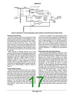
Figure 18 shows the step response of the COMP pin at a
fixed level. Before T1, the converter is in normal
steady−state operation. The inductor current provides a
portion of the PWM ramp through the current sense
amplifier. The PWM cycle ends when the sum of the current
ramp, the “partial” internal ramp voltage signal and offset
exceed the level of the COMP pin. At T1, the output current
increases and the output voltage sags. The next PWM cycle
begins and the cycle continues longer than previously while
the current signal increases enough to make up for the lower
R
V
C
time constant of the feedback components from
to the CSx pin.
CSx CSx
CORE
Including both current and voltage information in the
feedback signal allows the open loop output impedance of
the power stage to be controlled. When the average output
current is zero, the COMP pin will be:
voltage at the V pin and the cycle ends at T2. After T2, the
FB
output voltage remains lower than at light load and the
average current signal level (CSx output) is raised so that the
sum of the current and voltage signal is the same as with the
original load. In a closed loop system, the COMP pin would
move higher to restore the output voltage to the original
level.
V
+
V
@ 0 A ) Channel_Startup_Offset
COMP
OUT
) Int_Ramp ) G
@ Ext_Rampń2
CSA
Int_Ramp is the “partial” internal ramp value at the
corresponding duty cycle, Ext_Ramp is the peak−to−peak
external steady−state ramp at 0 A, G
is the current sense
CSA
amplifier gain (3.0 V/V) and the channel startup offset is
0.60 V. The magnitude of the Ext_Ramp can be calculated
from:
SWNODE
Ext_Ramp + D @ (V * V
IN
)ń(R
OUT
@ C
@ f )
CSx SW
CSx
V
FB
(V
OUT
)
For example, if V
at 0 A is set to 1.480 V with AVP
OUT
and the input voltage is 12.0 V, the duty cycle (D) will be
1.480/12.0 or 12.3%. Int_Ramp will be
100 mV/50% 12.3% = 25 mV. Realistic values for R
Internal Ramp
,
CSx
C
and f are 10 kW, 0.015 m F and 650 kHz. Using these
CSx
SW
CSA Out
and the previously mentioned formula, Ext_Ramp will be
15.0 mV.
COMP−Offset
CSA Out + Ramp + CS
V
+ 1.480 V ) 0.60 V ) 25 mV
) 2.65 VńV @ 15.0 mVń2
+ 2.125 Vdc.
COMP
REF
T1
T2
Figure 18. Open Loop Operation
If the COMP pin is held steady and the inductor current
changes, there must also be a change in the output voltage,
http://onsemi.com
16

 ONSEMI [ ONSEMI ]