NCP5316
APPLICATIONS INFORMATION
Overview
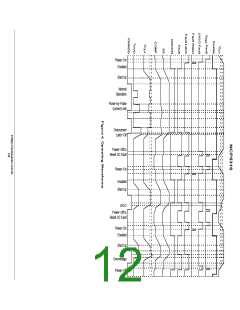
The NCP5316 controller uses six−phase, fixed−frequency,
Enhanced V architecture to measure and control currents in
2
The NCP5316 DC/DC controller from ON Semiconductor
2
was developed using the Enhanced V topology. Enhanced
individual phases. In six−phase mode, each phase is delayed
60° from the previous phase. Normally, GATEx transitions
to a high voltage at the beginning of each oscillator cycle.
Inductor current ramps up until the combination of the
current sense signal, the internal ramp and the output voltage
ripple trip the PWM comparator and bring GATEx low.
Once GATEx goes low, it will remain low until the
beginning of the next oscillator cycle. While GATEx is high,
2
2
V
combines the original V topology with peak
current−mode control for fast transient response and current
sensing capability. The addition of an internal PWM ramp
and implementation of fast−feedback directly from Vcore
has improved transient response and simplified design. This
controller can be adjusted to operate as a four−, five− or
six−phase controller, and can also be used in a one−, two− or
three−phase system. Differential current sensing provides
improved current sharing and easier layout. The NCP5316
includes Power Good (PWRGD), providing a highly
integrated solution to simplify design, minimize circuit
board area, and reduce overall system cost.
Two advantages of a multi−phase converter over a
single−phase converter are current sharing and increased
effective output frequency. Current sharing allows the designer
to use less inductance in each phase than would be required in
a single−phase converter. The smaller inductor will produce
larger ripple currents but the total per−phase power dissipation
is reduced because the RMS current is lower. Transient
response is improved because the control loop will measure
and adjust the current faster in a smaller output inductor.
Increased apparent output frequency is desirable because the
off− time and the ripple voltage of the multi−phase converter
will be less than that of a single−phase converter.
2
the Enhanced V loop will respond to line and load
variations. On the other hand, once GATEx is low, the loop
cannot respond until the beginning of the next PWM cycle.
2
Therefore, constant frequency Enhanced V will typically
respond to disturbances within the off−time of the converter.
2
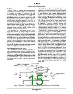
The Enhanced V architecture measures and adjusts the
output current in each phase. An additional differential input
(CSxN and CSxP) for inductor current information has been
2
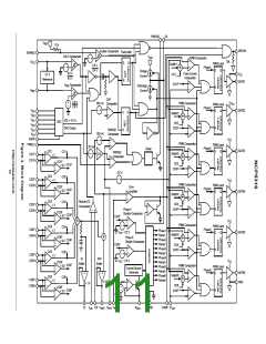
added to the V loop for each phase as shown in Figure 17.
The triangular inductor current is measured differentially
across RS, amplified by CSA and summed with the channel
startup offset, the internal ramp and the output voltage at the
non−inverting input of the PWM comparator. The purpose
of the internal ramp is to compensate for propagation delays
in the NCP5316. This provides greater design flexibility by
allowing smaller external ramps, lower minimum pulse
widths, higher frequency operation and PWM duty cycles
above 50% without external slope compensation. As the
sum of the inductor current and the internal ramp increase,
the voltage on the positive pin of the PWM comparator rises
and terminates the PWM cycle. If the inductor starts a cycle
with higher current, the PWM cycle will terminate earlier
providing negative feedback. The NCP5316 provides a
differential current sense input (CSxN and CSxP) for each
phase. Current sharing is accomplished by referencing all
phases to the same COMP pin, so that a phase with a larger
current signal will turn off earlier than a phase with a smaller
current signal.
Fixed Frequency Multi−Phase Control
In a multi−phase converter, multiple converters are
connected in parallel and are switched on at different times.
This reduces output current from the individual converters
and increases the apparent ripple frequency. Because several
converters are connected in parallel, output current can ramp
up or down faster than a single converter (with the same
value output inductor) and heat is spread among multiple
components.
x = 1, 2, 3, 4, 5 or 6
Lx
SWNODE
CSxP
CSxN
RLx
+
CSA
−
COx
RSx
Internal Ramp
V
FFB
V
OUT
“Fast−Feedback”
Connection
+
−
To PWM Latch Reset
Channel
Start−Up
Offset
(V
)
CORE
+
V
FB
−
PWM
COMP
E.A.
+
DAC
Out
COMP
+
Figure 17. Enhanced V2 Control Employing Resistive Current Sensing and Internal Ramp
http://onsemi.com
15

 ONSEMI [ ONSEMI ]