NCP3170
The ESR of the output capacitor creates a “zero” at the
determining phase margin. To start the design, a resistor
frequency as shown in Equation 39:
value should be chosen for R from which all other
1
components can be chosen. A good starting value is 24.9 kW.
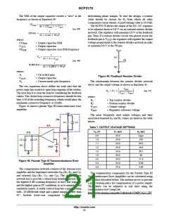
The NCP3170 allows the output of the DC−DC regulator
to be adjusted down to 0.8 V via an external resistor divider
network. The regulator will maintain 0.8 V at the feedback
pin. Thus, if a resistor divider circuit was placed across the
1
FZESR
+
³
2p COESR COUT
(eq. 39)
1
723 kHz +
2p 5 mW 44 mF
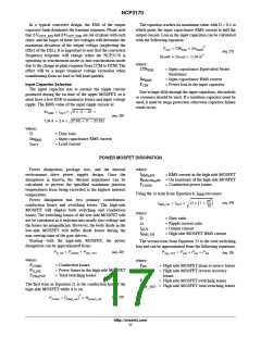
feedback pin to V
voltage proportional to the resistor divider network in order
to maintain 0.8 V at the FB pin.
, the regulator will regulate the output
OUT
where:
CO
= Output capacitor ESR
= Output capacitor
ESR
C
OUT
FZ
= Output capacitor zero ESR frequency
ESR
V
OUT
1
FP
+
³
R1
2p A COUT
FB
(eq. 40)
1
10.664 kHz +
2p 0.339 W 44 mF
R2
where:
A
= Un-scaled gain
= Output capacitor
= Current mode pole frequency
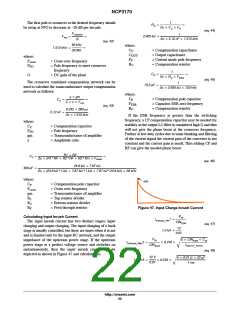
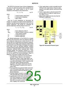
Figure 46. Feedback Resistor Divider
C
OUT
P
F
The relationship between the resistor divider network
above and the output voltage is shown in Equation 41:
The two equations above define the bode plot that the
power stage has created or open loop response of the system.
The next step is to close the loop by considering the feedback
values. The closed loop crossover frequency should be less
than 1/10 of the switching frequency, which would place the
maximum crossover frequency at 50 kHz.
VREF
ǒ
Ǔ
R2 + R1
(eq. 41)
VOUT * VREF
where:
R
R
= Top resistor divider
= Bottom resistor divider
= Output voltage
1
2
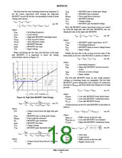
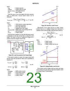
Figure 45 shows a pseudo Type III transconductance error
amplifier.
V
OUT
V
REF
= Regulator reference voltage
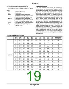
The most frequently used output voltages and their
associated standard R and R values are listed in the table
below.
1
2
ZIN
CF
R1
R2
IEA
Table 7. OUTPUT VOLTAGE SETTINGS
V
O
(V)
R (kW)
1
R (kW)
2
ZFB
0.8
1.0
1.1
1.2
1.5
1.8
2.5
3.3
5.0
24.9
24.9
24.9
24.9
24.9
24.9
24.9
24.9
24.9
Open
100
CC
RC
CP
+
66.5
49.9
28.7
20
VREF
−
11.8
8.06
4.64
Figure 45. Pseudo Type III Transconductance Error
Amplifier
The compensation network consists of the internal error
amplifier and the impedance networks Z (R , R , and C )
IN
1
2
F
The compensation components for the Pseudo Type III
Transconductance Error Amplifier can be calculated using
the method described below. The method serves to provide
a good starting place for compensation of a power supply.
The values can be adjusted in real time using the
compensation tool CompCalc
and external Z (R , C , and C ). The compensation
FB
C
C
P
network has to provide a closed loop transfer function with
the highest 0 dB crossing frequency to have fast response
and the highest gain in DC conditions, so as to minimize load
regulation issues. A stable control loop has a gain crossing
with −20 dB/decade slope and a phase margin greater than
45°. Include worst-case component variations when
http://www.onsemi.com/pub/Collateral/COMPCALC.ZIP
http://onsemi.com
21

 ONSEMI [ ONSEMI ]