NCP3170
Compensation Network
The body diode losses can be approximated as:
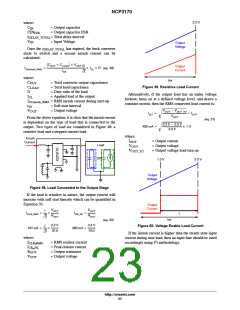
To create a stable power supply, the compensation
network around the transconductance amplifier must be
used in conjunction with the PWM generator and the power
stage. Since the power stage design criteria is set by the
application, the compensation network must correct the
overall output to ensure stability. The NCP3170 is a current
mode regulator and as such there exists a voltage loop and
a current loop. The current loop causes the inductor to act
like a current source which governs most of the
characteristics of current mode control. The output inductor
and capacitor of the power stage form a double pole but
because the inductor is treated like a current source in closed
loop, it becomes a single pole system. Since the feedback
loop is controlling the inductor current, it is effectively like
having a current source feeding a capacitor; therefore the
pole is controlled by the load and the output capacitance. A
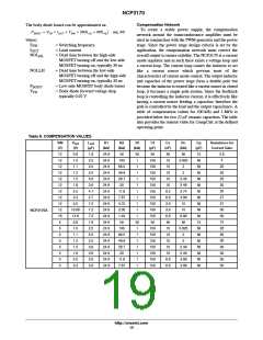
table of compensation values for 500 kHz and 1 MHz is
provided below for two 22 mF ceramic capacitors. The table
also provides the resistor value for CompCalc at the defined
operating point.
ǒ
Ǔ
(eq. 34)
PBODY + VFD IOUT FSW NOLLH ) NOLHL
where:
F
I
= Switching frequency
= Load current
SW
OUT
NOL
= Dead time between the high-side
MOSFET turning off and the low-side
MOSFET turning on, typically 30 ns
= Dead time between the low-side
MOSFET turning off and the high-side
MOSFET turning on, typically 30 ns
= Low-side MOSFET body diode losses
= Body diode forward voltage drop
typically 0.92 V
HL
NOLLH
P
BODY
V
FD
Table 6. COMPENSATION VALUES
VIN
(V)
V
L
R1
R2
Rf
Cf
Cc
Rc
Cp
Resistance for
Current Gain
out
out
(V)
0.8
1.0
1.1
1.2
1.5
1.8
2.5
3.3
5.0
10.68
14.8
0.8
1.0
1.1
1.2
1.5
1.8
2.5
3.3
(mF)
1.8
2.5
2.5
2.5
3.6
3.6
4.7
4.7
7.2
7.2
7.2
1.8
2.5
2.5
2.5
3.6
3.6
3.6
3.6
(kW)
(kW)
(kW)
(pF)
(nF)
(kW)
(pF)
12
12
12
12
12
12
12
12
12
12
18
5
24.9
24.9
24.9
24.9
24.9
24.9
24.9
24.9
24.9
24.9
24.9
24.9
24.9
24.9
24.9
24.9
24.9
24.9
24.9
NI
NI
1
1
1
1
1
1
1
1
1
1
NI
1
1
1
1
1
1
1
NI
NI
15
10
10
10
10
8.2
6.8
3.9
3.9
6.8
NI
NI
0.825
2
15
NI
NI
NI
NI
NI
NI
NI
NI
NI
NI
15
NI
NI
NI
NI
NI
NI
NI
3.6
4
100
66.5
49.9
28.7
20
150
150
150
150
150
150
150
150
150
150
NI
20
20
20
20
25
27
27
30
30
15
28
30
30
30
30
50
50
2
2.49
2.49
3.74
4.99
10
11.8
7.87
4.75
2.05
1.43
NI
10
NCP3170A
6.98
NI
5
100
66.5
49.9
28.7
20
150
150
150
150
150
150
150
15
10
10
10
10
6.8
6.8
0.825
2
5
5
2
5
2.49
2.49
4.99
4.99
5
5
11.8
7.87
5
http://onsemi.com
19

 ONSEMI [ ONSEMI ]